Unlike optical microscopes, scanning electron microscopes (SEMs) use electrons rather than light rays to generate images of the specimen being studied. And to understand how SEMs work, it’s important to grasp the concept of backscattered electrons (BSEs).
BSEs are high-energy electrons used to obtain high-resolution images that show the distribution of various elements that make up a sample.
To picture how BSEs function, think of an asteroid that circles the earth but then drifts back into space without getting captured by the earth’s gravitational pull. In a similar way, when the sample is bombarded with electrons, some of the negatively charged electrons won’t be captured by the pull of the positive nucleus. Instead, they’ll be reflected or “backscattered” out of the sample.

Schematic of an electron being backscattered by the interaction with the atom nuclei.
Production of backscattered electrons
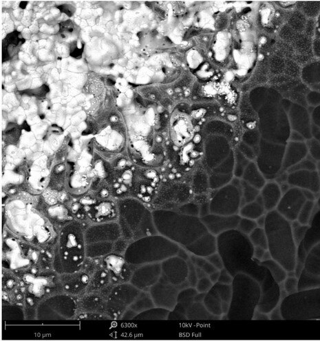
The production of backscattered electrons differs based on the weight of the element. Typically, heavier elements, because of their bigger nuclei, can deflect incident electrons more strongly than lighter elements. Hence, heavy elements like silver, which has the atomic number Z=47, appear bright in an SEM image compared to lighter elements, such as silicon, which has the atomic number Z=14, because more backscattered electrons are emitted from the sample surface.

SEM image of a solar cell, where the heavier element silver appears bright compared to the dark area of the lighter element silicon.
Detection of backscattered electrons
The detection of BSEs is often carried out by detectors that consist of a semiconductor material, typically silicon, placed directly above the sample. Electrons that hit the detectors excite the silicon electrons, creating an electron-hole pair. Semiconductor detectors are only sensitive to electrons with high energy, which is why they’re used are to detect backscattered electrons.
The free electrons and pairs generated from backscattered electrons can be separated before their recombination, generating a current. This current can be measured by an electronic circuit, which is eventually converted into a high-resolution image containing information about the elemental makeup of the sample.
High resolution BSE imaging in SEM
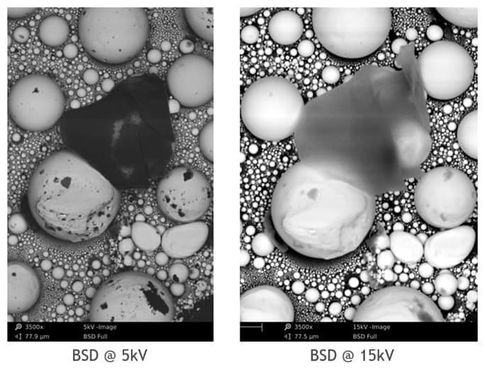
The quality of BSE images can be manipulated depending on the researcher’s goals. When a higher acceleration voltage is used, for example, the penetration depth increases, making it harder to see thin film layers on the sample surface. Therefore, if the researcher’s goal is to examine these surface layers, it’s critical to use a primary beam with a low acceleration voltage.

BSE images of a tin ball sample with carbon dirt flakes taken with 5kV and 15kV beam acceleration voltages. Since the dirt flakes are very shallow, they become less visible when a 15kV acceleration voltage is used.
Backscattered electrons are used to obtain high-resolution images of the elements present in a sample. By having a clear understanding of how BSEs work and the different factors that can be manipulated, users can obtain the high-quality images needed to advance their research.
To learn more about backscattered electrons and scanning electron microscopy, fill out this form to speak with an expert.
Erik Luyk is a marketing communications specialist at Thermo Fisher Scientific.

Leave a Reply