Search Thermo Fisher Scientific
- Contact Us
- Quick Order
-
Don't have an account ? Create Account
Search Thermo Fisher Scientific
Thermo Scientific NEXS Software goes far beyond a CAD viewer and stage driver by facilitating fault isolation, failure analysis, sample preparation and circuit edit. NEXS Software enables diverse workflows by providing CAD connectivity with Thermo Scientific analytical equipment.
NEXS Software directly reads/displays the mask data and drives the system stage accurately to fault or edit locations.
Technical specifications
Database file formats supported
Thermo Scientific equipment supported
Innovation starts with research and development. Learn more about solutions to help you understand innovative structures and materials at the atomic level.
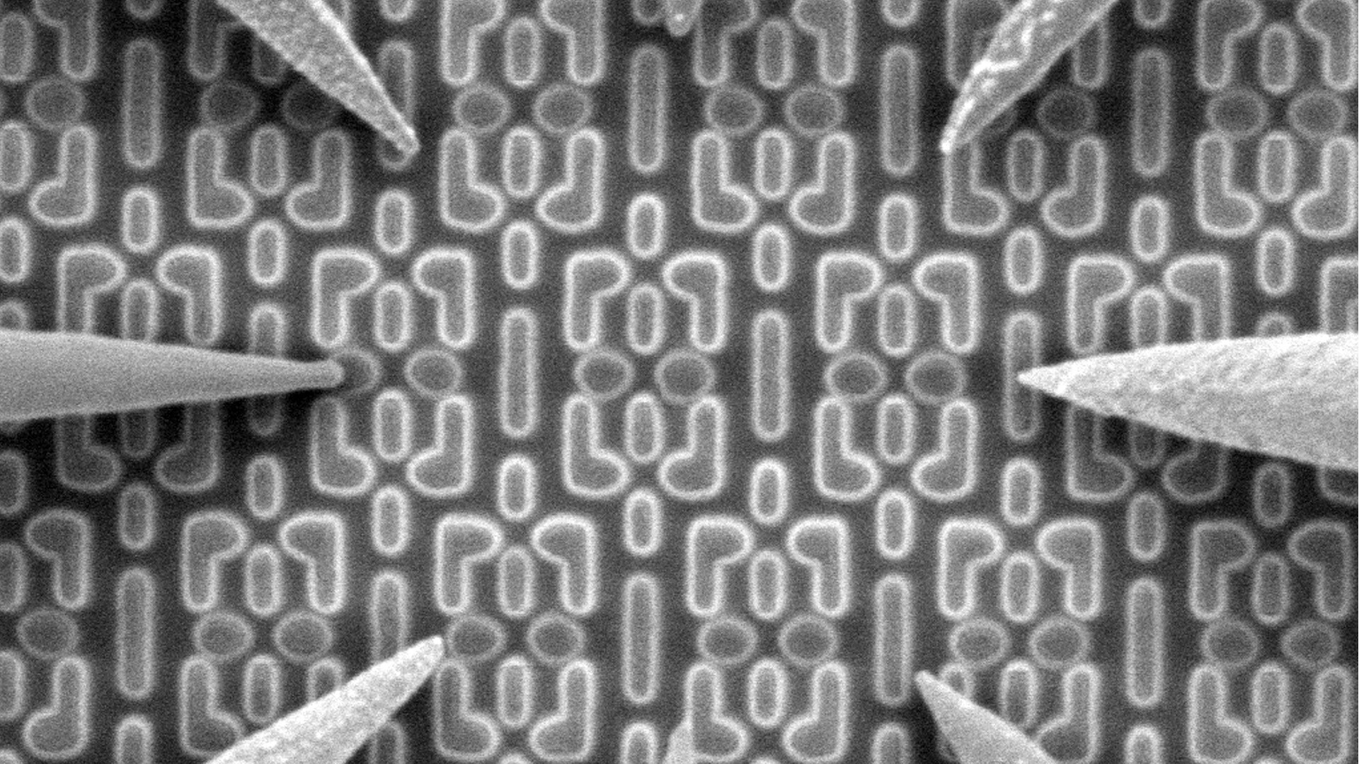
Complex semiconductor device structures result in more places for defects to hide. Learn more about failure analysis solutions to isolate, analyze, and repair defects.
Optical Fault Isolation
Increasingly complex designs complicate fault and defect isolation in semiconductor manufacturing. Optical fault isolation techniques allow you to analyze the performance of electrically active devices to locate critical defects that cause device failure.
Circuit Edit
Advanced, dedicated circuit edit and nanoprototyping solutions, which combine novel gas-delivery systems with a broad portfolio of chemistries and focused ion beam technology, offer unparalleled control and precision for semiconductor device development.
To ensure optimal system performance, we provide you access to a world-class network of field service experts, technical support, and certified spare parts.

