Search Thermo Fisher Scientific
Semiconductor Analysis
Semiconductor TEM Metrology
Metrology with transmission electron microscopy for fast, automated, and highly precise measurements, accelerating time-to-data and maximizing yields.
Join the Conversation
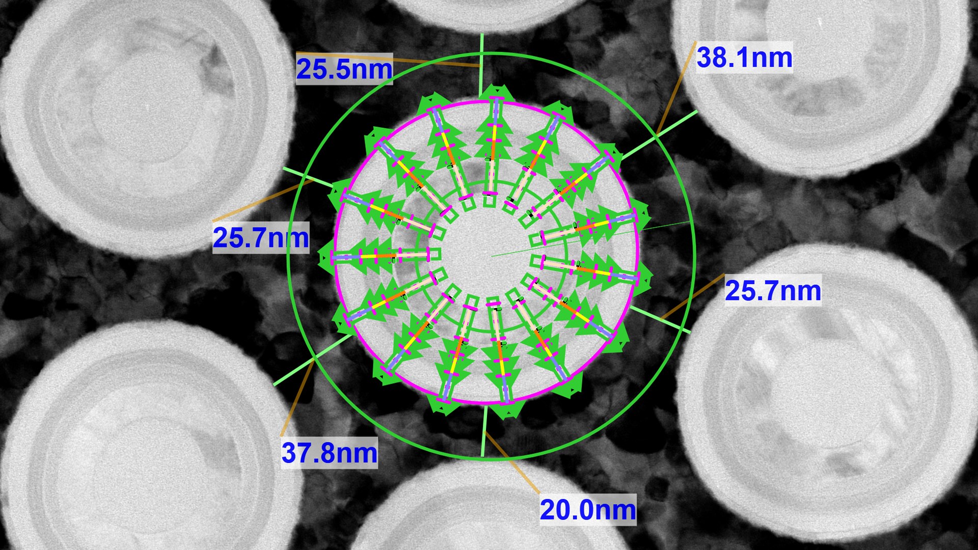
Semiconductor devices are becoming more complex due to the demand for faster speeds, shorter time-to-yield, and time-to-market. Scanning transmission electron microscopy (S)TEM metrology has become a necessary element of all leading-edge wafer fabrication workflows, since highly specific measurements are needed to generate statistically relevant data with sub-angstrom accuracy. This data allows manufacturers to calibrate toolsets, diagnose failure mechanisms, and optimize overall process yield.
Thermo Fisher Scientific offers metrology workflows that are flexible enough to enable manual, semi-automated, or even fully automated solutions, depending on your needs. The Thermo Scientific Metrios AX System is the first TEM designed to provide the fast, precise measurements that semiconductor manufacturers need to develop and control their wafer fabrication processes. Learn more by visiting the Metrios product page below.


Semiconductor research and development
Innovation starts with research and development. Learn more about solutions to help you understand innovative structures and materials at the atomic level.

Semiconductor materials characterization
Many factors impact yield, performance, and reliability. Learn more about solutions to characterize physical, structural, and chemical properties.

Semiconductor metrology
Manufacturing today’s complex semiconductors requires exact process controls. Learn more about advanced metrology and analysis solutions to accelerate yield learnings.
Semiconductor Materials and Device Characterization
As semiconductor devices shrink and become more complex, new designs and structures are needed. High-productivity 3D analysis workflows can shorten device development time, maximize yield, and ensure that devices meet the future needs of the industry.
Electron microscopy services for
semiconductors
To ensure optimal system performance, we provide you access to a world-class network of field service experts, technical support, and certified spare parts.


