Search Thermo Fisher Scientific
- Order Status
- Quick Order
-
Don't have an account ? Create Account
Search Thermo Fisher Scientific
The sixth-generation of Thermo Scientific Phenom ProX G6 Desktop SEM fills the gap between light microscopy and floor-model SEM analysis, thus expanding the capabilities of research facilities. It offers fast, high-resolution imaging in addition to an integrated energy-dispersive X-ray diffraction (EDS) detector for robust, easy-to-use, rapid elemental analysis.
The Phenom Pro Desktop SEM can be used to relieve the burden of routine analysis for common samples from floor-model SEM instruments. Instrument configuration and the sample loading mechanism ensure quick imaging with minimal time spent tuning between experiments.
Facility users of any experience level can quickly begin producing high-quality results with the Phenom Pro Desktop SEM. Its long-lifetime CeB6 source offers high brightness while requiring low maintenance.
It's high stability and small form factor allow the instrument to be used in practically any lab environment; more simply put, it does not require specialized infrastructure or expert oversight.

| Light optical magnification |
|
| Electron optical magnification range |
|
| Resolution |
|
| Digital zoom |
|
| Light optical navigation camera |
|
| Acceleration voltages |
|
| Vacuum modes |
|
| Detector |
|
| Sample size |
|
| Sample height |
|
Want to unlock the great power of scanning electron microscopy without having to compromise on usability? Enhance your knowledge on Scanning Electron Microscopy and find out how Desktop SEM can optimally support your research in our Phenom Desktop SEM blogs.
Product Development Engineer Luigi Raspolini explains everything that is new on the Thermo Scientific Phenom ProX G6 - The Desktop SEM with EDS capability for robust, effortless, and versatile elemental and SEM analysis.
Testimonial from Professor Sir Colin Humphreys, University of Cambridge.
Watch this webinar to learn about:
This on-demand webinar has been designed to help you decide which SEM best meets your unique needs. We present an overview of Thermo Fisher Scientific SEM technology for multi-user research labs and focus on how these wide-ranging solutions deliver performance, versatility, in situ dynamics and faster time to results. Watch this webinar if you are interested in:
Discover How GMSI Advanced Their Materials Development with a Desktop SEM
Discover how DSM Improved their Material Research with a Desktop SEM
Measuring Thrombin Activity at Synapse with the Desktop SEM
Research on the Structure of Nonwoven Textiles at Technical University Liberec with the Desktop SEM
Modern industry demands high throughput with superior quality, a balance that is maintained through robust process control. SEM and TEM tools with dedicated automation software provide rapid, multi-scale information for process monitoring and improvement.
Quality control and assurance are essential in modern industry. We offer a range of EM and spectroscopy tools for multi-scale and multi-modal analysis of defects, allowing you to make reliable and informed decisions for process control and improvement.
Novel materials are investigated at increasingly smaller scales for maximum control of their physical and chemical properties. Electron microscopy provides researchers with key insight into a wide variety of material characteristics at the micro- to nano-scale.
Innovation starts with research and development. Learn more about solutions to help you understand innovative structures and materials at the atomic level.
Manufacturing today’s complex semiconductors requires exact process controls. Learn more about advanced metrology and analysis solutions to accelerate yield learnings.
Complex semiconductor device structures result in more places for defects to hide. Learn more about failure analysis solutions to isolate, analyze, and repair defects.
Many factors impact yield, performance, and reliability. Learn more about solutions to characterize physical, structural, and chemical properties.
_Technique_800x375_144DPI.jpg)
EDS Elemental Analysis
Thermo Scientific Phenom Elemental Mapping Software provides fast and reliable information on the distribution of chemical elements within a sample.
_Technique_800x375_144DPI.jpg)
3D EDS Tomography
Modern materials research is increasingly reliant on nanoscale analysis in three dimensions. 3D characterization, including compositional data for full chemical and structural context, is possible with 3D EM and energy dispersive X-ray spectroscopy.

Atomic-Scale Elemental Mapping with EDS
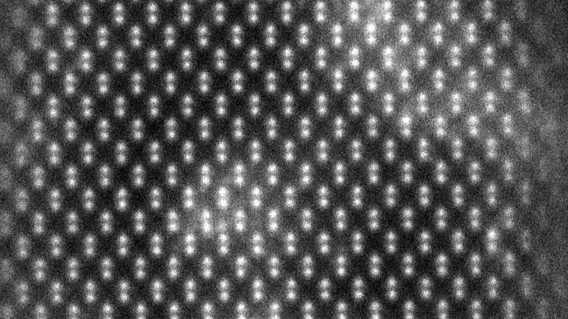
Atomic-resolution EDS provides unparalleled chemical context for materials analysis by differentiating the elemental identity of individual atoms. When combined with high-resolution TEM, it is possible to observe the precise organization of atoms in a sample.

Imaging Hot Samples
Studying materials in real-world conditions often involves working at high temperatures. The behavior of materials as they recrystallize, melt, deform, or react in the presence of heat can be studied in situ with scanning electron microscopy or DualBeam tools.

In Situ experimentation
Direct, real-time observation of microstructural changes with electron microscopy is necessary to understand the underlying principles of dynamic processes such as recrystallization, grain growth, and phase transformation during heating, cooling, and wetting.

Multi-scale analysis
Novel materials must be analyzed at ever higher resolution while retaining the larger context of the sample. Multi-scale analysis allows for the correlation of various imaging tools and modalities such as X-ray microCT, DualBeam, Laser PFIB, SEM and TEM.
SEM Metrology
Scanning electron microscopy provides accurate and reliable metrology data at nanometer scales. Automated ultra-high-resolution SEM metrology enables faster time-to-yield and time-to-market for memory, logic, and data storage applications.
Semiconductor Analysis and Imaging
Thermo Fisher Scientific offers scanning electron microscopes for every function of a semiconductor lab, from general imaging tasks to advanced failure analysis techniques requiring precise voltage-contrast measurements.
_Technique_800x375_144DPI.jpg)
EDS Elemental Analysis
Thermo Scientific Phenom Elemental Mapping Software provides fast and reliable information on the distribution of chemical elements within a sample.
_Technique_800x375_144DPI.jpg)
3D EDS Tomography
Modern materials research is increasingly reliant on nanoscale analysis in three dimensions. 3D characterization, including compositional data for full chemical and structural context, is possible with 3D EM and energy dispersive X-ray spectroscopy.

Atomic-Scale Elemental Mapping with EDS
Atomic-resolution EDS provides unparalleled chemical context for materials analysis by differentiating the elemental identity of individual atoms. When combined with high-resolution TEM, it is possible to observe the precise organization of atoms in a sample.

Imaging Hot Samples
Studying materials in real-world conditions often involves working at high temperatures. The behavior of materials as they recrystallize, melt, deform, or react in the presence of heat can be studied in situ with scanning electron microscopy or DualBeam tools.

In Situ experimentation
Direct, real-time observation of microstructural changes with electron microscopy is necessary to understand the underlying principles of dynamic processes such as recrystallization, grain growth, and phase transformation during heating, cooling, and wetting.

Multi-scale analysis
Novel materials must be analyzed at ever higher resolution while retaining the larger context of the sample. Multi-scale analysis allows for the correlation of various imaging tools and modalities such as X-ray microCT, DualBeam, Laser PFIB, SEM and TEM.
SEM Metrology
Scanning electron microscopy provides accurate and reliable metrology data at nanometer scales. Automated ultra-high-resolution SEM metrology enables faster time-to-yield and time-to-market for memory, logic, and data storage applications.
Semiconductor Analysis and Imaging
Thermo Fisher Scientific offers scanning electron microscopes for every function of a semiconductor lab, from general imaging tasks to advanced failure analysis techniques requiring precise voltage-contrast measurements.
To ensure optimal system performance, we provide you access to a world-class network of field service experts, technical support, and certified spare parts.
