Search Thermo Fisher Scientific
- Order Status
- Quick Order
-
Don't have an account ? Create Account
Search Thermo Fisher Scientific
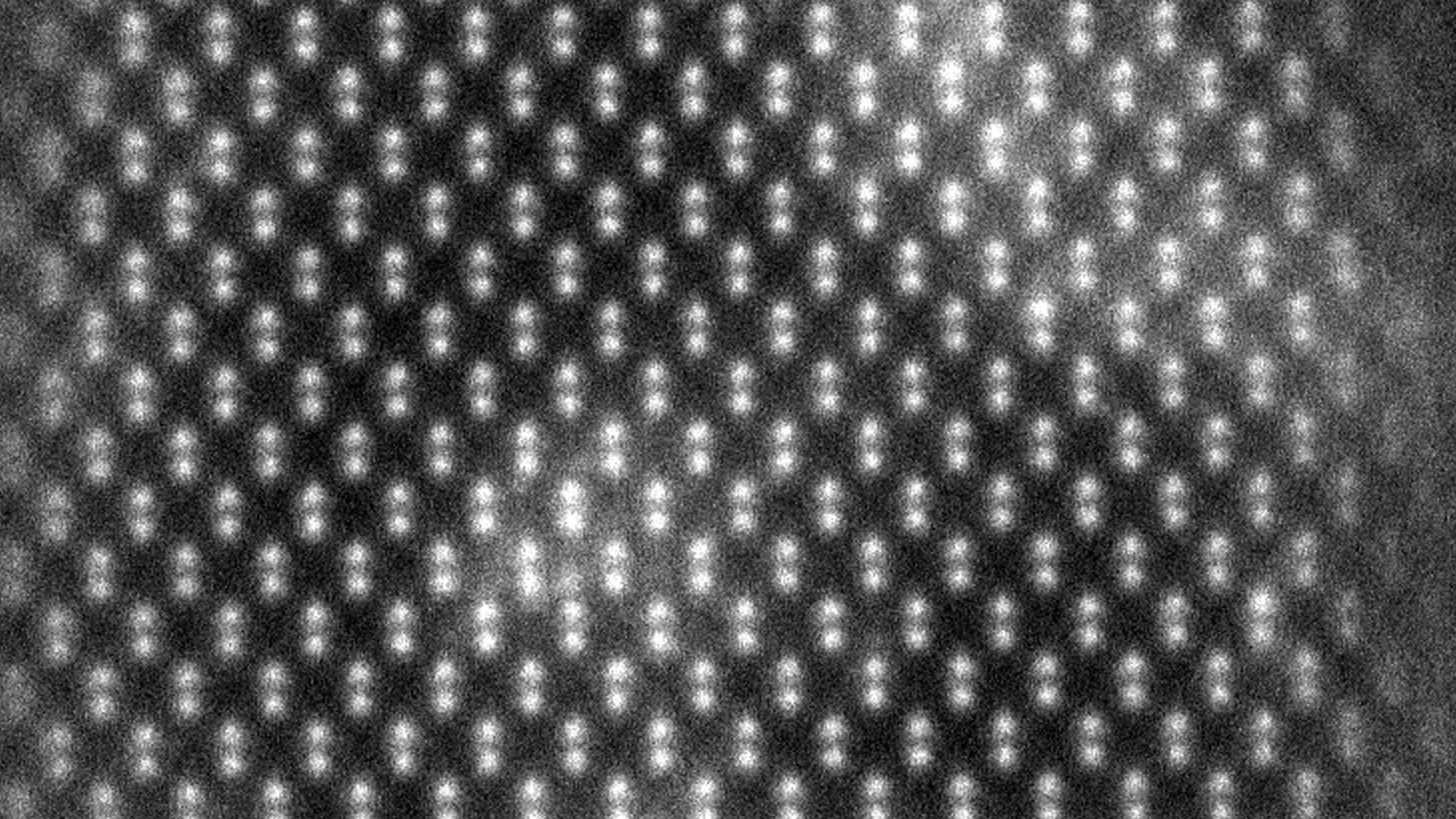
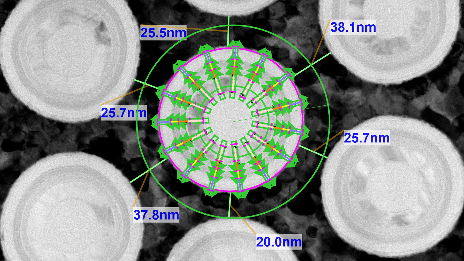
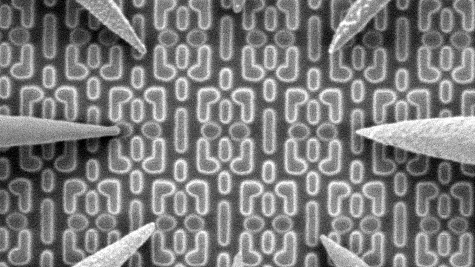
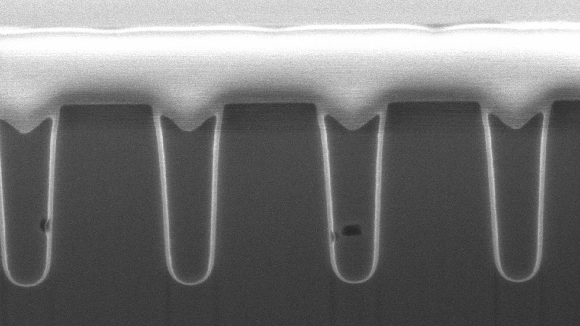
Advanced (scanning) transmission electron microscopy (S)TEM have become a necessary part of all leading-edge wafer-fabrication workflows due to an increasing demand for high-quality, rapid analysis and imaging of complex structures. Semiconductor designers need analytical tools that offer excellent flexibility and stability, as well as high-resolution imaging, in order to properly analyze and optimize device performance. (S)TEM characterization allows manufacturers to calibrate toolsets, diagnose failure mechanisms, and optimize overall process yields.
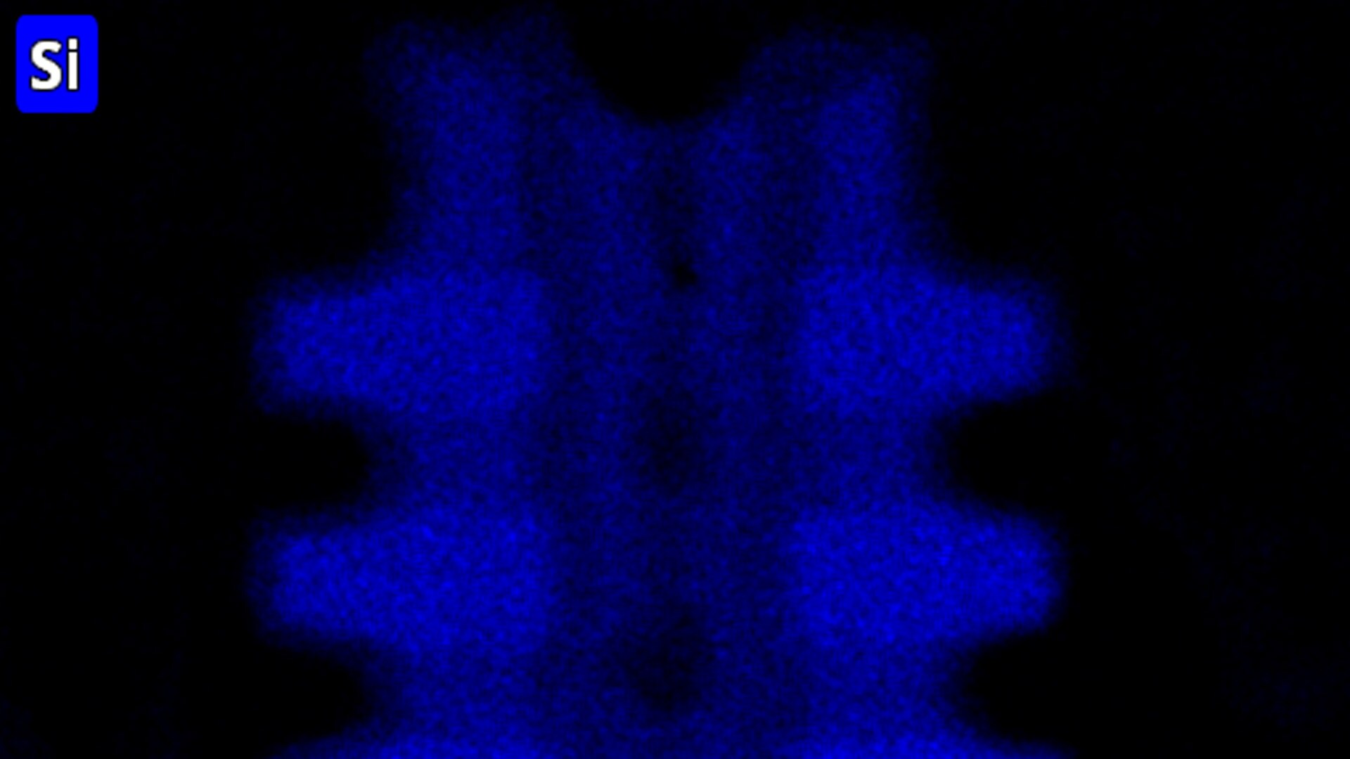
Beyond imaging, a range of techniques are available on (S)TEM instrumentation that are critical for semiconductor device characterization, including; electron diffraction, for crystal orientation mapping or strain analysis, energy-dispersive X-ray spectroscopy (EDS), for qualitative or quantitative composition analysis, and electron energy-loss spectroscopy (EELS), for compositional and chemical information. Additionally, advanced imaging techniques, such as electron holography, tomography, Lorentz imaging and (integrated) differential phase-contrast (iDPC/DPC) imaging, are also available and are now routinely used in semiconductor labs.
Thermo Fisher Scientific is the world leader in TEM workflows for metrology, analysis, and pathfinding in semiconductor devices thanks to an uncompromising combination of high-resolution imaging and high analytical performance. Click through to the appropriate product pages below to learn more.
Innovation starts with research and development. Learn more about solutions to help you understand innovative structures and materials at the atomic level.
Manufacturing today’s complex semiconductors requires exact process controls. Learn more about advanced metrology and analysis solutions to accelerate yield learnings.
Complex semiconductor device structures result in more places for defects to hide. Learn more about failure analysis solutions to isolate, analyze, and repair defects.
Many factors impact yield, performance, and reliability. Learn more about solutions to characterize physical, structural, and chemical properties.
Novel architectures and materials pose new challenges. Learn how to pinpoint faults and characterize materials, structures, and interfaces.
Display technologies are evolving to improve display quality and light conversion efficiency. Learn how metrology, failure analysis, and characterization solutions provide insights.
As semiconductor devices shrink and become more complex, new designs and structures are needed. High-productivity 3D analysis workflows can shorten device development time, maximize yield, and ensure that devices meet the future needs of the industry.
To ensure optimal system performance, we provide you access to a world-class network of field service experts, technical support, and certified spare parts.
