Search Thermo Fisher Scientific
- Order Status
- Quick Order
-
Don't have an account ? Create Account
Search Thermo Fisher Scientific
For scientists to advance their understanding of complex samples and develop innovative materials, they must have access to robust, precise instrumentation capable of correlating form and function, as well as resolving space, time and frequency.
Thermo Fisher Scientific introduces the Thermo Scientific Spectra 200 (S)TEM, the high-throughput, aberration-corrected, (scanning) transmission electron microscope for all materials science applications.
All Spectra 200 (S)TEM's are delivered on new platforms designed to offer an unprecedented level of mechanical stability and highest imaging quality though passive and (optional) active vibration isolation.
The system is housed in a fully re-designed enclosure with a built-in on-screen display for convenient specimen loading and removal. For the first time, full modularity and upgradeability can be offered between uncorrected and single-corrected configurations with variable heights, allowing maximum flexibility for different room configurations.
The Spectra 200 (S)TEM can be powered by a new-cold field emission gun (X-CFEG). The X-CFEG has extremely high brightness (>>1.0 x 10⁸ A/m2/Sr/V*), low energy spread, and can be operated from 30 – 200 kV. This provides high-resolution STEM imaging with high probe currents for high-throughput, fast acquisition STEM analytics. With the powerful combination of X-CFEG and S-CORR probe aberration corrector, sub-Angstrom STEM imaging with over 1000 pA of probe current can be routinely achieved.
Further, probe currents can be flexibly tuned from <1 pA up to the nA range with fine control of the gun and condenser optics, all with minimum impact on the probe aberrations, so that the widest range of specimens and experiments can be accommodated (see the MOF example in the Panther STEM detection section).
As with all cold field emission sources, the sharp tip requires a periodic regeneration (called flashing) to maintain the probe current. With the X-CFEG, the tip only requires flashing once per working day, a process that takes less than a minute. There is no measurable impact on the probe aberrations even in the highest resolution imaging conditions and the daily tip flashing process has no impact on the tip lifetime.
Tip flashing on the X-CFEG: 60 pm resolution at 200 kV is maintained before and after a tip flashing without adjustment of the optics. The process takes less than one minute and is required only once per working day and has no impact on the lifetime of the tip.
This new generation X-CFEG also produces enough total beam current (>14 nA) to support standard TEM imaging experiments (e.g. in situ) with large parallel probes, making it a uniquely all-purpose, yet high-performance, C-FEG.
The combination of enhanced mechanical stability, the latest 5th order S-CORR probe aberration correction and the X-CFEG, gives the Spectra 200 (S)TEM high-resolution, high-contrast STEM imaging capability for all accelerating voltages. Additionally, Spectra 200 (S)TEM retains the wide gap S-TWIN objective lens as standard from the Themis product line, to ensure customers have a pole gap with “room to do more” without compromising on spatial resolution. In the images below, 48 pm resolution is shown on a wide gap S-TWIN Spectra 200 (S)TEM at 200 kV.
Adding to ease of use, the Spectra 200 (S)TEM includes smart software algorithms to quickly, reproducibly and reliably correct up to 4th order aberrations in the STEM probe (Auto S-CORR) and optimize 1st and 2nd order aberrations on any specimen (OptiSTEM+). Auto S-CORR can therefore be used on a weekly basis to maintain high-order aberrations and OptiSTEM+ can be used daily to optimize image quality without the need of a standard specimen or manual tuning.
Si [110] and GaN [212] taken on a Spectra 200 (S)TEM showing the specified resolution on a wide gap analytical S-TWIN pole piece (green circle) and achievable resolution (red circles). At 60 kV, 96 pm resolution is specified and at 200 kV, 60 pm is specified with an achievable resolution <48 pm.
The Spectra 200 (S)TEM offers STEM resolution specifications of 60 pm at 200 kV, 96 pm at 60 kV and 125 pm at 30 kV. For a full list of specifications, please refer to the Spectra 200 (S)TEM datasheet.
STEM imaging on the Spectra 200 (S)TEM has been re-imagined with the Panther STEM detection system, which includes a new data acquisition architecture and two new, solid state, eight-segment ring and disk STEM detectors (16 segments in total). The new detector geometry offers access to advanced STEM imaging capability combined with the sensitivity to measure single electrons.
The entire signal is optimized and tuned to provide unprecedented signal-to-noise imaging capability with extremely low doses to facilitate imaging of beam sensitive materials. Additionally, the completely redeveloped data acquisition infrastructure can combine different individual detector segments, with the future possibility of combining detector segments in arbitrary ways, generating new STEM imaging methods and revealing information that is not present in conventional STEM techniques. The architecture is also scalable and provides an interface to synchronize multiple STEM and spectroscopic signals.
The Spectra 200 (S)TEM can be configured with an electron microscope pixel array detector (EMPAD) or a Thermo Scientific Ceta Camera with speed enhancement to collect 4D STEM data sets.
The EMPAD is capable of 30-300 kV and provides a high dynamic range (1:1,000,000 e- between pixels), high signal-to-noise ratio (1/140 e-), and high speed (1100 frames per second) on a 128 x 128 pixel array, which makes it the optimal detector for 4D STEM applications. (E.g. Applications where the details of the central and diffracted beams need to be analyzed simultaneously, as in the ptychography image below.)
More details can be found in the EMPAD datasheet.
The EMPAD detector can be used for a wide variety of applications. On the left, it is used to extend spatial resolution (0.39 Å) beyond the aperture limited resolution at low accelerating voltages (80 kV) in a bi-layer of the 2D material MoS2 ( Jiang, Y. et al. Nature 559, 343–349, 2018) . On the right, it is used to independently image dark field reflections, revealing the complex microstructure of the precipitates in a superalloy (Sample courtesy Professor G. Burke, University of Manchester).
The Ceta Camera with speed enhancement offers an alternative for 4D STEM applications where a greater number of pixels is required and when EDX analysis needs to be combined with each point in the STEM scan. This solution provides higher resolution diffraction patterns (up to 512 x 512 pixel resolution), suited for applications such as strain measurement.
The Spectra 200 (S)TEM has been configured to be a STEM analytics powerhouse. The extreme brightness and low energy spread of the X-CFEG, the latest generation, 5th order S-CORR probe corrector, the wide gap (S-TWIN or X-TWIN) pole piece with a portfolio of large solid angle and symmetric EDS detectors and the built-in EDX quantification engine in Thermo Scientific Velox Software makes STEM EDX on Spectra 200 (S)TEM fast, easy and quantifiable.
The Thermo Scientific EDX detector portfolio provides a choice of detector geometries to suit your experimental requirements and optimize EDX results. Both configurations have a symmetric design (see below), producing quantifiable data. Note that holder shadowing as a function of tilt is compensated in both detector configurations via built-in Velox Software functionality.
The Spectra 200 (S)TEM can be configured with either Super-X (for spectrum cleanliness and quantification) or Dual-X (for the largest solid angle and high-throughput STEM EDX mapping).
The Super-X detector system provides a highly collimated solid angle of 0.7 Sr and a Fiori number greater than 4000. It is designed for STEM EDX experiments where spectral cleanliness and quantification are critical.
The Dual-X detector system provides a solid angle of 1.76 Sr and a Fiori number greater than 2000. It is designed for high-throughput STEM EDX experiments such as EDS tomography or where signal yield is low and fast mapping is critical.
In the example below, the DyScO3 perovskite system is examined with the Dual-X detectors. The ultra-high brightness (>>1.0 x 10⁸ A/m2/Sr/V*) of the X-CFEG and the resolving power of the S-CORR probe corrector are used to deliver a probe to the specimen with 150 pA of current and size <80 pm. With these high-brightness probe conditions, EDX mapping can be done rapidly with high sampling and high SNR, resulting in, for the first time, sub-Å spatial information in a single elemental, raw, and unfiltered EDX map. A fast Fourier transform of the Sc map shows up to 90 pm resolution.
DyScO3 specimen investigated with the powerful combination of ultra-high brightness X-CFEG, S-CORR and the large solid angle (1.76 Sr) of the Dual-X detectors, resulting in high signal-to-noise ratio, atomic resolution (up to 90 pm), unfiltered EDX maps (Sample courtesy Professor L.F. Kourkoutis, Cornell University).
Electron energy loss spectroscopy on Spectra 200 (S)TEM has also been accelerated by the ultra-high brightness (>>1.0 x 10⁸ A/m2/Sr/V*) and intrinsically high energy resolution (<0.4 eV) of the X-CFEG which are delivered simultaneously in the STEM probe.
In the figure below, a probe with narrow energy spread (0.36 eV) and high current (480 pA) high spatial resolution (65 pm) provides ideal conditions to collect the Dy, Sc and O core loss edges with high energy resolution, signal to noise ratio and spatial resolution in the STEM image.
DyScO3 specimen investigated with a Spectra 200 (S)TEM. The combined ultra-high brightness of the X-CFEG, intrinsically low energy spread of the source (<0.40 eV) and resolving power of the S-CORR results in high signal-to-noise ratio, Sc, O and Dy core loss edges with a sub-70 pm STEM probe (Sample courtesy Professor L.F. Kourkoutis, Cornell University).
| Spectra 200 (S)TEM |
|
| Source |
|
| Analytics and detectors |
|
| Available detector options |
|
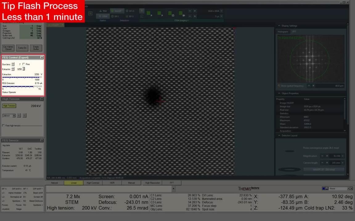
Tip flashing on the X-CFEG: 60 pm resolution at 200 kV is maintained before and after a tip flashing without adjustment of the optics. The process takes < 1 min, and is required only once per working day and has no impact on the lifetime of the tip.
The Spectra 200 (S)TEM can be configured with Dual-X for the largest solid angle and high-throughput STEM EDX mapping.
The Spectra 200 (S)TEM can be configured with Super-X for spectrum cleanliness and quantification.
Thermo Fisher Scientific introduces the Spectra 200 (S)TEM – the high-throughput, aberration-corrected, scanning transmission electron microscope for all materials science applications.
Register below to watch our recorded webinar and learn more about how the Spectra 200 (S)TEM delivers the highest-quality data for all applications. With an ultra-high-brightness X-CFEG source and a wide-gap pole piece with “room to do more,” it is the ultimate atomic-resolution materials-characterization tool.
Modern industry demands high throughput with superior quality, a balance that is maintained through robust process control. SEM and TEM tools with dedicated automation software provide rapid, multi-scale information for process monitoring and improvement.
Quality control and assurance are essential in modern industry. We offer a range of EM and spectroscopy tools for multi-scale and multi-modal analysis of defects, allowing you to make reliable and informed decisions for process control and improvement.
Novel materials are investigated at increasingly smaller scales for maximum control of their physical and chemical properties. Electron microscopy provides researchers with key insight into a wide variety of material characteristics at the micro- to nano-scale.
Novel architectures and materials pose new challenges. Learn how to pinpoint faults and characterize materials, structures, and interfaces.
Display technologies are evolving to improve display quality and light conversion efficiency. Learn how metrology, failure analysis, and characterization solutions provide insights.

Energy Dispersive Spectroscopy
Energy dispersive spectroscopy (EDS) collects detailed elemental information along with electron microscopy images, providing critical compositional context for EM observations. With EDS, chemical composition can be determined from quick, holistic surface scans down to individual atoms.
_Technique_800x375_144DPI.jpg)
3D EDS Tomography
Modern materials research is increasingly reliant on nanoscale analysis in three dimensions. 3D characterization, including compositional data for full chemical and structural context, is possible with 3D EM and energy dispersive X-ray spectroscopy.

Atomic-Scale Elemental Mapping with EDS
Atomic-resolution EDS provides unparalleled chemical context for materials analysis by differentiating the elemental identity of individual atoms. When combined with high-resolution TEM, it is possible to observe the precise organization of atoms in a sample.
_Technique_800x375_144DPI.jpg)
EDS Elemental Analysis
Thermo Scientific Phenom Elemental Mapping Software provides fast and reliable information on the distribution of chemical elements within a sample.

Electron Energy Loss Spectroscopy
Materials science research benefits from high-resolution EELS for a wide range of analytical applications. This includes high-throughput, high signal-to-noise-ratio elemental mapping, as well as probing of oxidation states and surface phonons.

In Situ experimentation
Direct, real-time observation of microstructural changes with electron microscopy is necessary to understand the underlying principles of dynamic processes such as recrystallization, grain growth, and phase transformation during heating, cooling, and wetting.

Particle analysis
Particle analysis plays a vital role in nanomaterials research and quality control. The nanometer-scale resolution and superior imaging of electron microscopy can be combined with specialized software for rapid characterization of powders and particles.

Multi-scale analysis
Novel materials must be analyzed at ever higher resolution while retaining the larger context of the sample. Multi-scale analysis allows for the correlation of various imaging tools and modalities such as X-ray microCT, DualBeam, Laser PFIB, SEM and TEM.

The Automated NanoParticle Workflow (APW) is a transmission electron microscope workflow for nanoparticle analysis, offering large area, high resolution imaging and data acquisition at the nanoscale, with on-the-fly processing.
Energy Dispersive Spectroscopy
Energy dispersive spectroscopy (EDS) collects detailed elemental information along with electron microscopy images, providing critical compositional context for EM observations. With EDS, chemical composition can be determined from quick, holistic surface scans down to individual atoms.
3D EDS Tomography
Modern materials research is increasingly reliant on nanoscale analysis in three dimensions. 3D characterization, including compositional data for full chemical and structural context, is possible with 3D EM and energy dispersive X-ray spectroscopy.
Atomic-Scale Elemental Mapping with EDS
Atomic-resolution EDS provides unparalleled chemical context for materials analysis by differentiating the elemental identity of individual atoms. When combined with high-resolution TEM, it is possible to observe the precise organization of atoms in a sample.
EDS Elemental Analysis
Thermo Scientific Phenom Elemental Mapping Software provides fast and reliable information on the distribution of chemical elements within a sample.
Electron Energy Loss Spectroscopy
Materials science research benefits from high-resolution EELS for a wide range of analytical applications. This includes high-throughput, high signal-to-noise-ratio elemental mapping, as well as probing of oxidation states and surface phonons.
In Situ experimentation
Direct, real-time observation of microstructural changes with electron microscopy is necessary to understand the underlying principles of dynamic processes such as recrystallization, grain growth, and phase transformation during heating, cooling, and wetting.
Particle analysis
Particle analysis plays a vital role in nanomaterials research and quality control. The nanometer-scale resolution and superior imaging of electron microscopy can be combined with specialized software for rapid characterization of powders and particles.
Multi-scale analysis
Novel materials must be analyzed at ever higher resolution while retaining the larger context of the sample. Multi-scale analysis allows for the correlation of various imaging tools and modalities such as X-ray microCT, DualBeam, Laser PFIB, SEM and TEM.
The Automated NanoParticle Workflow (APW) is a transmission electron microscope workflow for nanoparticle analysis, offering large area, high resolution imaging and data acquisition at the nanoscale, with on-the-fly processing.
To ensure optimal system performance, we provide you access to a world-class network of field service experts, technical support, and certified spare parts.

 images of silicon.")
 images of GaN and silicon.")

 images of SrTiO3.")

 image of MoS2.")


 images of silicon.")
 images of GaN and silicon.")

 images of SrTiO₃.")

 image of MoS₂.")


TEM")


