Search Thermo Fisher Scientific
- Order Status
- Quick Order
-
Don't have an account ? Create Account
Search Thermo Fisher Scientific
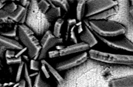
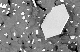
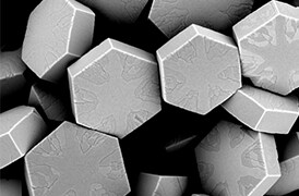
The new Thermo Scientific Helios 5 DualBeam builds on the high-performance imaging and analysis capabilities of the industry-leading Helios DualBeam family. It is carefully designed to meet the needs of materials science researchers and engineers for a wide range of focused ion beam scanning electron microscopy (FIB-SEM) use cases – even on the most challenging samples.
The Helios 5 DualBeam redefines the standard in high-resolution imaging with high materials contrast; fast, easy, and precise high-quality sample preparation for (S)TEM imaging and atom probe tomography (APT) as well as the high-quality subsurface and 3D characterization. Building on the proven capabilities of the Helios DualBeam family, additional advancements to the new Helios 5 DualBeam were designed to ensure the system is optimized for a variety of manual or automated workflows. Those improvements include:
The Thermo Scientific Helios 5 DualBeam is part of the fifth generation of the industry-leading Helios DualBeam family. It is carefully designed to meet the needs of scientists and engineers, combining the innovative Elstar electron column for extreme high-resolution imaging and the high materials contrast with the superior Thermo Scientific Tomahawk Ion Column for the fast, easy, and precise high-quality sample preparation. In addition to the advanced electron and ion optics, the Helios 5 DualBeam incorporates a suite of state of-the-art technologies that enables simple and consistent high-resolution (S)TEM and atom probe tomography (APT) sample preparation, as well as the high-quality subsurface and 3D characterization, even on the most challenging samples.
Site-specific sample preparation for (S)TEM and APT analysis using the high-throughput Thermo Scientific Tomahawk Ion Column or the Thermo Scientific Phoenix Ion Column with unmatched low-voltage performance.
Fast and easy, fully automated, unattended, multi-site in situ and ex situ TEM sample preparation and cross-sectioning using optional AutoTEM 5 Software.
For users with any experience level using best-in-class Thermo Scientific Elstar Electron Column featuring Thermo Scientific SmartAlign and FLASH technologies.
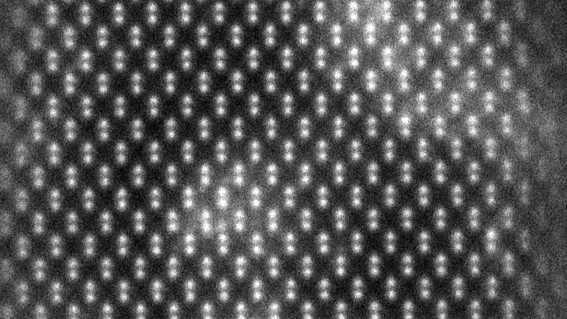
Reveal the finest details with the next-generation UC+ monochromator technology with higher current, enabling sub-nanometer performance at low energies.
Sharp, refined and charge-free contrast obtained from up to six integrated in-column and below-the-lens detectors.
The high-quality, multi-modal subsurface and 3D information with the precise region-of-interest targeting using optional Thermo Scientific Auto Slice & View 4 (AS&V4) Software.
Fast, accurate and precise milling and deposition of complex structures with critical dimensions of less than 10 nm.
Tailored to individual application needs thanks to the high stability and accuracy of the 150-mm piezo stage or the flexibility of the 110-mm stage, as well as the in-chamber Thermo Scientific Nav-Cam Camera.
Based on integrated sample cleanliness management and dedicated imaging modes such as DCFI and SmartScan Modes.
The Thermo Scientific Helios 5 FX configuration offers a high productivity workflow with its unique, in-situ, 3Å resolution STEM capability.
To view the specifications of the Helios 5 HX DualBeam and Helios 5 FX DualBeam, download the datasheet found in the documents section.
| Helios 5 CX | Helios 5 HP | Helios 5 UX | Helios 5 HX | Helios 5 FX | ||
| Workhorse preparation and XHR SEM imaging | Ultimate sample preparation (TEM lamellae, APT) | Angstrom-scale STEM imaging and sample preparation | ||||
| SEM | Resolution | 20 eV – 30 keV | 20 eV – 30 keV | |||
| Landing energy | 0.6 nm @ 15 keV 1.0 nm @ 1 keV | 0.6 nm @ 2 keV 0.7 nm @ 1 keV 1.0 nm @ 500 eV | ||||
| STEM | Resolution @ 30 keV | 0.7 nm | 0.6 nm | 0.3 nm | ||
| FIB preparation processes | Max material removal | 100 nA | 100 nA | 65 nA | ||
| Optimal final polish | 2 kV | 500 V | ||||
| TEM sample preparation | Sample thickness | 50 nm | 15 nm | 7 nm | ||
| Automation | No | Yes | Yes | |||
| Sample handling | Travel | 110 x 110 x 65 mm | 100 x 100 x 65 mm | 150 x 150 x 10 mm | 100 x 100 x 20 mm | 100 x 100 x 20 mm + 5 axis (S)TEM Compustage |
| Loadlock | Manual Quickloader | Automated | Manual Quickloader | Automated | Auto + Auto insert/extract STEM rod | |
| Helios 5 CX | Helios 5 UC | Helios 5 UX | ||
| Ion optics | Tomahawk HT Ion Column with superior high-current performance | Phoenix Ion Column with superior high-current and low-voltage performance | ||
| Ion beam current range | 1 pA – 100 nA | 1 pA – 65 nA | ||
| Accelerating voltage range | 500 V – 30 kV | 500 V – 30 kV | ||
| Max. horizontal field width | 0.9 mm at beam coincidence point | 0.7 mm at beam coincidence point | ||
| Minimum source lifetime | 1,000 hours | 1,000 hours | ||
| Two-stage differential pumping Time-of-flight (TOF) correction 15-position aperture strip | Two-stage differential pumping Time-of-flight (TOF) correction 15-position aperture strip | |||
| Electron optics | Elstar ultra-high-resolution field emission SEM column | Elstar extreme high-resolution field emission SEM column | ||
| Magnetic immersion objective lens | Magnetic immersion objective lens | |||
| High-stability Schottky field emission gun to provide stable high-resolution analytical currents | High-stability Schottky field emission gun to provide stable high-resolution analytical currents | |||
| Electron beam resolution | At optimum working distance (WD) | 0.6 nm at 30 kV STEM 0.6 nm at 15 kV 1.0 nm at 1 kV 0.9 nm at 1 kV with beam deceleration* | 0.6 nm at 30 kV STEM 0.7 nm at 1 kV 1.0 nm at 500 V (ICD) | |
| At coincident point | 0.6 nm at 15 kV 1.5 nm at 1 kV with beam deceleration* and DBS* | 0.6 nm at 15 kV 1.2 nm at 1 kV | ||
| Electron beam parameter space | Electron beam current range | 0.8 pA to 176 nA | 0.8 pA to 100 nA | |
| Accelerating voltage range | 200 V – 30 kV | 350 V – 30 kV | ||
| Landing energy range | 20 eV – 30 keV | 20 eV – 30 keV | ||
| Maximum horizontal field width | 2.3 mm at 4 mm WD | 2.3 mm at 4 mm WD | ||
| Detectors | Elstar in-lens SE/BSE detector (TLD-SE, TLD-BSE) | |||
| Elstar in-column SE/BSE detector (ICD)* | ||||
| Elstar in-column BSE detector (MD)* | ||||
| Everhart-Thornley SE detector (ETD) | ||||
| IR camera for viewing sample/column | ||||
| High-performance in-chamber electron and ion detector (ICE) for secondary ions (SI) and electrons (SE)* | ||||
| Thermo Scientific In-chamber Nav-Cam Camera for sample navigation* | ||||
| Retractable, low-voltage, high-contrast, directional, solid-state backscatter electron detector (DBS)* | ||||
| Retractable STEM 3+ detector with BF/ DF/ HAADF segments* | ||||
| Integrated beam current measurement | ||||
| Stage and sample | Stage | Flexible 5-axis motorized stage | High-precision five-axis motorized stage with Piezo-driven XYR axis | |
| XY range | 110 mm | 150 mm | ||
| Z range | 65 mm | 10 mm | ||
| Rotation | 360° (endless) | 360° (endless) | ||
| Tilt range | -15° to +90° | -10° to +60° | ||
| Max sample height | Clearance 85 mm to eucentric point | Clearance 55 mm to eucentric point | ||
| Max sample weight | 500 g in any stage position Up to 5 kg at 0° tilt (some restrictions apply) | 500 g (including sample holder) | ||
| Max sample size | 110 mm with full rotation (larger samples possible with limited rotation) | 150 mm with full rotation (larger samples possible with limited rotation) | ||
| Compucentric rotation and tilt | Compucentric rotation and tilt | |||
* Available as an option, configuration dependent
To support semiconductor manufacturing needs, Thermo Fisher Scientific continues to bring new capabilities to our industry-leading failure analysis, metrology and characterization solutions.
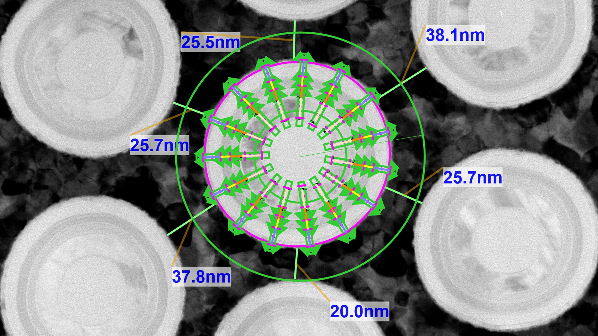
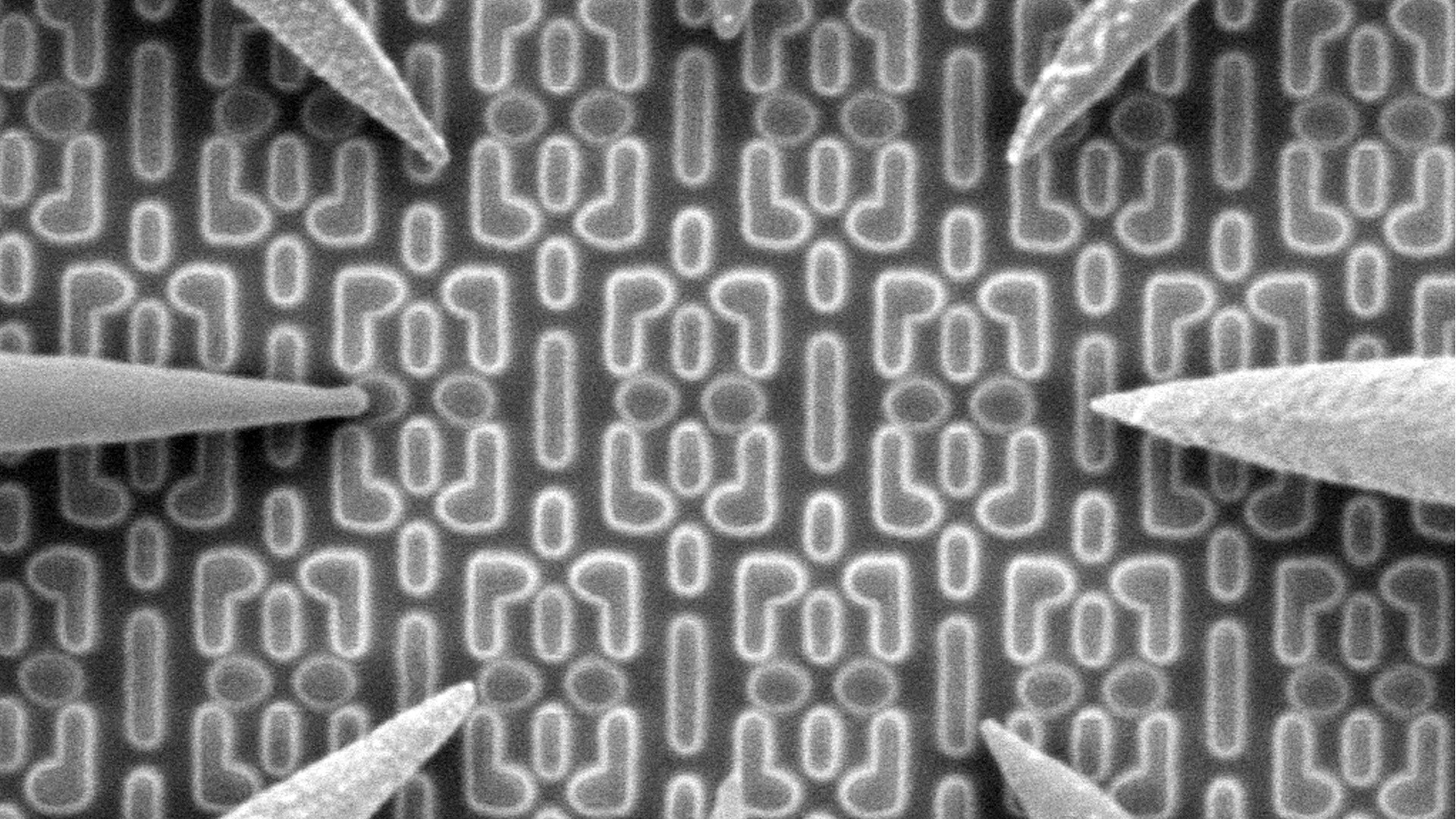
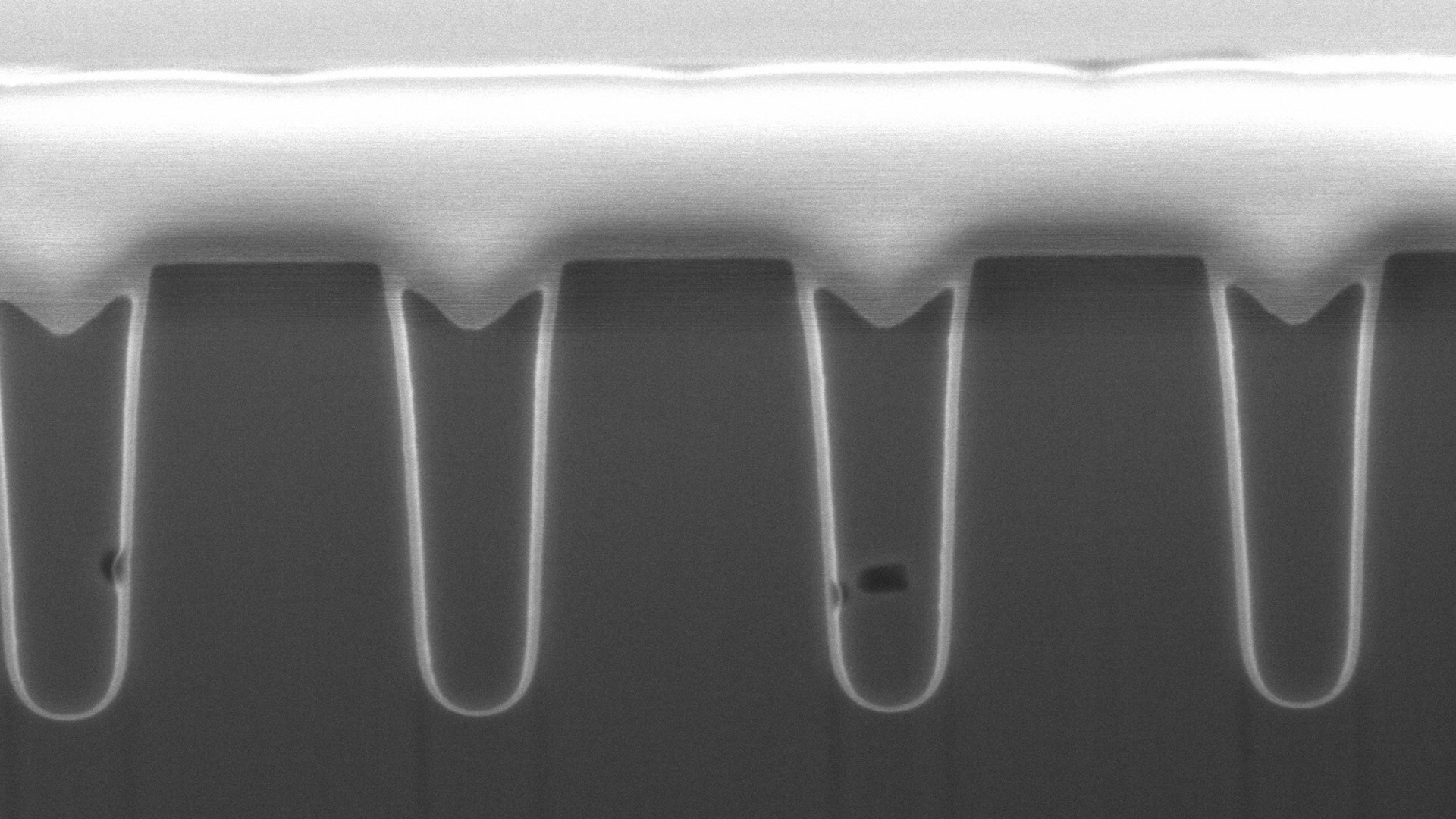
In our Thermo Fisher Scientific PFA Demo Days, we showcase our latest innovations for sample preparation and FinFET logic circuit delayering.
The new Thermo Scientific Helios 5 DualBeam builds on the high-performance imaging and analysis capabilities of the industry-leading Helios DualBeam family.
Register for our recorded webinar (~17 minutes) and learn how additional advancements to the new Helios 5 were designed to ensure the system is optimized for a variety of manual or automated workflows.
Register for our live webinar and learn how leading research labs are using our new Thermo Scientific Helios 5 Laser PFIB and Thermo Scientific Helios 5 Hydra DualBeam to advance their materials characterization.
Modern industry demands high throughput with superior quality, a balance that is maintained through robust process control. SEM and TEM tools with dedicated automation software provide rapid, multi-scale information for process monitoring and improvement.
Quality control and assurance are essential in modern industry. We offer a range of EM and spectroscopy tools for multi-scale and multi-modal analysis of defects, allowing you to make reliable and informed decisions for process control and improvement.
Novel materials are investigated at increasingly smaller scales for maximum control of their physical and chemical properties. Electron microscopy provides researchers with key insight into a wide variety of material characteristics at the micro- to nano-scale.
Innovation starts with research and development. Learn more about solutions to help you understand innovative structures and materials at the atomic level.
Manufacturing today’s complex semiconductors requires exact process controls. Learn more about advanced metrology and analysis solutions to accelerate yield learnings.
Complex semiconductor device structures result in more places for defects to hide. Learn more about failure analysis solutions to isolate, analyze, and repair defects.
Many factors impact yield, performance, and reliability. Learn more about solutions to characterize physical, structural, and chemical properties.
Novel architectures and materials pose new challenges. Learn how to pinpoint faults and characterize materials, structures, and interfaces.
Display technologies are evolving to improve display quality and light conversion efficiency. Learn how metrology, failure analysis, and characterization solutions provide insights.

(S)TEM Sample Preparation
DualBeam microscopes enable the preparation of high-quality, ultra-thin samples for (S)TEM analysis. Thanks to advanced automation, users with any experience level can obtain expert-level results for a wide range of materials.

3D Materials Characterization
Development of materials often requires multi-scale 3D characterization. DualBeam instruments enable serial sectioning of large volumes and subsequent SEM imaging at nanometer scale, which can be processed into high-quality 3D reconstructions of the sample.

Nanoscale Prototyping
As technology continues to miniaturize, the demand for nanoscale devices and structures is ever increasing. 3D nanoprototyping with DualBeam instruments helps you to quickly design, create, and inspect micro- and nanoscale functional prototypes.

APT Sample Preparation
Atom probe tomography (APT) provides atomic-resolution 3D compositional analysis of materials. Focused ion beam (FIB) microscopy is an essential technique for high-quality, orientation, and site-specific sample preparation for APT characterization.

Cross-sectioning
Cross sectioning provides extra insight by revealing sub-surface information. DualBeam instruments feature superior focused ion beam columns for high-quality cross sectioning. With automation, unattended high-throughput processing of samples is possible.

In Situ experimentation
Direct, real-time observation of microstructural changes with electron microscopy is necessary to understand the underlying principles of dynamic processes such as recrystallization, grain growth, and phase transformation during heating, cooling, and wetting.

Multi-scale analysis
Novel materials must be analyzed at ever higher resolution while retaining the larger context of the sample. Multi-scale analysis allows for the correlation of various imaging tools and modalities such as X-ray microCT, DualBeam, Laser PFIB, SEM and TEM.
Circuit Edit
Advanced, dedicated circuit edit and nanoprototyping solutions, which combine novel gas-delivery systems with a broad portfolio of chemistries and focused ion beam technology, offer unparalleled control and precision for semiconductor device development.
Semiconductor TEM Imaging and Analysis
Thermo Scientific transmission electron microscopes offer high-resolution imaging and analysis of semiconductor devices, enabling manufacturers to calibrate toolsets, diagnose failure mechanisms, and optimize overall process yields.
Sample Preparation of Semiconductor Devices
Thermo Scientific DualBeam systems provide accurate TEM sample preparation for atomic-scale analysis of semiconductor devices. Automation and advanced machine learning technologies produce high-quality samples, at the correct location, and a low cost per sample.
Semiconductor Analysis and Imaging
Thermo Fisher Scientific offers scanning electron microscopes for every function of a semiconductor lab, from general imaging tasks to advanced failure analysis techniques requiring precise voltage-contrast measurements.
Device Delayering
Shrinking feature size, along with advanced design and architecture, results in increasingly challenging failure analysis for semiconductors. Damage-free delayering of devices is a critical technique for the detection of buried electrical faults and failures.

(S)TEM Sample Preparation
DualBeam microscopes enable the preparation of high-quality, ultra-thin samples for (S)TEM analysis. Thanks to advanced automation, users with any experience level can obtain expert-level results for a wide range of materials.

3D Materials Characterization
Development of materials often requires multi-scale 3D characterization. DualBeam instruments enable serial sectioning of large volumes and subsequent SEM imaging at nanometer scale, which can be processed into high-quality 3D reconstructions of the sample.

Nanoscale Prototyping
As technology continues to miniaturize, the demand for nanoscale devices and structures is ever increasing. 3D nanoprototyping with DualBeam instruments helps you to quickly design, create, and inspect micro- and nanoscale functional prototypes.

APT Sample Preparation
Atom probe tomography (APT) provides atomic-resolution 3D compositional analysis of materials. Focused ion beam (FIB) microscopy is an essential technique for high-quality, orientation, and site-specific sample preparation for APT characterization.

Cross-sectioning
Cross sectioning provides extra insight by revealing sub-surface information. DualBeam instruments feature superior focused ion beam columns for high-quality cross sectioning. With automation, unattended high-throughput processing of samples is possible.

In Situ experimentation
Direct, real-time observation of microstructural changes with electron microscopy is necessary to understand the underlying principles of dynamic processes such as recrystallization, grain growth, and phase transformation during heating, cooling, and wetting.

Multi-scale analysis
Novel materials must be analyzed at ever higher resolution while retaining the larger context of the sample. Multi-scale analysis allows for the correlation of various imaging tools and modalities such as X-ray microCT, DualBeam, Laser PFIB, SEM and TEM.
Circuit Edit
Advanced, dedicated circuit edit and nanoprototyping solutions, which combine novel gas-delivery systems with a broad portfolio of chemistries and focused ion beam technology, offer unparalleled control and precision for semiconductor device development.
Semiconductor TEM Imaging and Analysis
Thermo Scientific transmission electron microscopes offer high-resolution imaging and analysis of semiconductor devices, enabling manufacturers to calibrate toolsets, diagnose failure mechanisms, and optimize overall process yields.
Sample Preparation of Semiconductor Devices
Thermo Scientific DualBeam systems provide accurate TEM sample preparation for atomic-scale analysis of semiconductor devices. Automation and advanced machine learning technologies produce high-quality samples, at the correct location, and a low cost per sample.
Semiconductor Analysis and Imaging
Thermo Fisher Scientific offers scanning electron microscopes for every function of a semiconductor lab, from general imaging tasks to advanced failure analysis techniques requiring precise voltage-contrast measurements.
Device Delayering
Shrinking feature size, along with advanced design and architecture, results in increasingly challenging failure analysis for semiconductors. Damage-free delayering of devices is a critical technique for the detection of buried electrical faults and failures.
To ensure optimal system performance, we provide you access to a world-class network of field service experts, technical support, and certified spare parts.


