Search Thermo Fisher Scientific
- Order Status
- Quick Order
-
Don't have an account ? Create Account
Search Thermo Fisher Scientific
Thermo Fisher Scientific provides a range of electron microscopy and spectroscopy solutions that make understanding 2D materials faster and more productive. Being able to correlate analysis across different techniques, either on a single platform like the Thermo Scientific Nexsa G2 Surface Analysis System or across spectroscopy and microscopy tools with the CISA or nanoscale workflows, builds a more complete picture of the structure and chemistry of a sample quickly and easily.
Our high-performance instruments offer easy automation of key procedures and can accelerate key research tasks including measuring layer thickness using X-ray photoelectron spectroscopy and Raman spectroscopy, identifying structural defects at the atomic scale using scanning transmission electron microscopy, and identifying structure and chemical state using the CISA workflow.
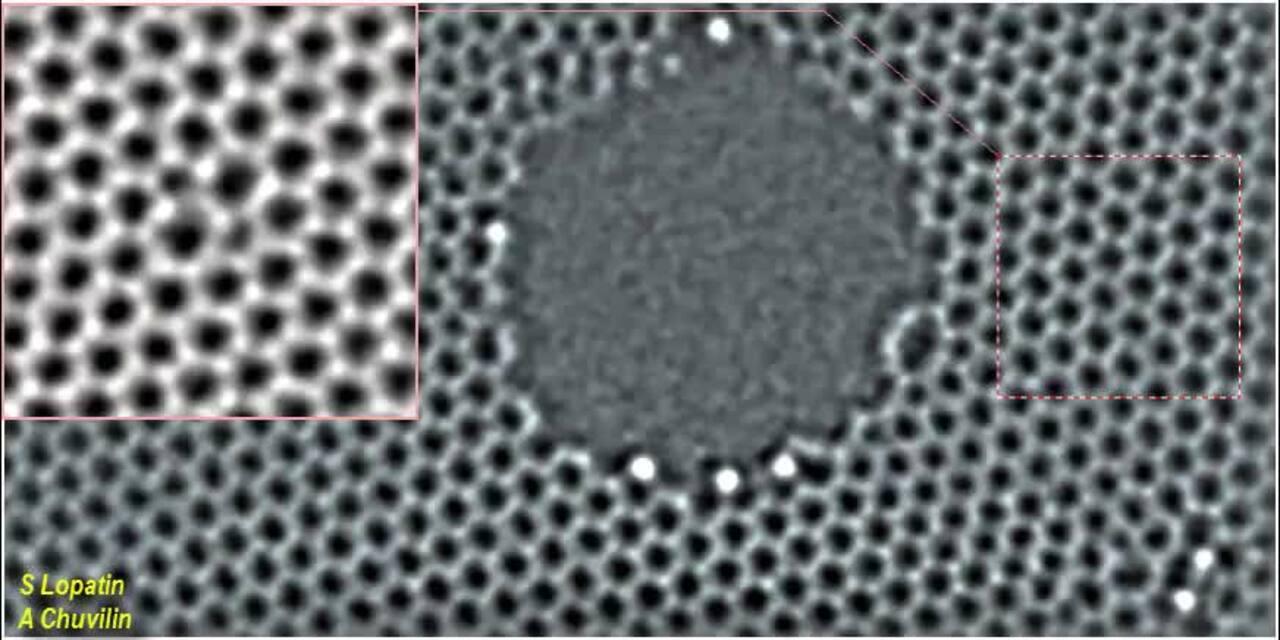
Transmission electron microscopy (TEM), or in particular low-kV scanning transmission electron microscopy, can image 2D materials at atomic resolution. This capacity is, however, significantly impacted by radiolysis. Beam damage-free imaging can often only be achieved at low accelerating voltages below the knock-on damage threshold (typically under 60 kV). At these low values, resolution-limiting aberrations can substantially undermine imaging efforts.
Monochromation of the electron beam or the use of a cold field emission gun have proven to be reliable ways to reduce chromatic blurring. A probe corrector can further improve signal by reducing, or potentially even eliminating, aberrations at low accelerating voltages.
Thermo Fisher Scientific combines monochromation and probe correction in the Thermo Scientific Spectra S/TEM product line, which is ideally suited to imaging 2D materials. With the Spectra S/TEM, accelerating voltages as low as 30 kV are possible due to the superior correction capability of the Thermo Scientific S-CORR Probe Corrector along with the Thermo Scientific CETCOR Image Corrector, which compensates for spherical aberrations.
 Extreme-low-dose imaging (166 e- / Å2) of the metal organic framework (MOF) UiO 66. A Spectra 300 S/TEM was used in combination with iDPC to image atomic-level details in this highly dose-sensitive material. Image courtesy of Professor Y. Han, King Abdullah University of Science and Technology.
Scanning electron microscopy (SEM) allows for high-resolution imaging of materials at the nanoscale, providing valuable insights into their surface morphology, topography, and composition. SEM can distinguish a monolayer of graphene from multiple layers by the contrast in the image. Moreover, the growth of 2D materials can be studied in-situ using an environmental SEM.
X-ray photoelectron spectroscopy provides information about the chemical composition, electronic structure, and bonding states of materials. By irradiating a sample with X-rays and measuring the emitted photoelectrons, the technique can determine the elemental composition, chemical state, and electronic state of the surface layers of 2D materials. This technique is particularly useful for characterizing surface chemistry and functionalizing 2D materials because it can identify the presence of impurities, contaminants, or chemical modifications.
The ultra-thin nature of 2D materials, and the importance of chemical modification in tuning their performance to meet the requirements of an application, means that X-ray photoelectron spectroscopy and other surface analysis techniques are ideally suited to their characterization.
 Left: XPS SnapMap of the MoS2 surface recorded at the location indicated by the red box (inset, top right). Right: Raman spectra collected at P1 and MoS2. The P1 splitting peaks were compared to a reference spectrum of bulk MoS2; this suggests that the material is likely present in an ultra-thin layer.
X-ray photoelectron spectroscopy, or electron spectroscopy for chemical analysis (ESCA), is a common surface characterization tool for examining non-stick cookware coatings, thin-film electronics, and bioactive surfaces.
X-ray photoelectron spectroscopy spectra are obtained by irradiating a solid surface with a beam of X-rays and measuring the kinetic energy of electrons that are emitted through the photoelectric effect from the top 1 to 10 nm of the material. A photoelectron spectrum is recorded by counting ejected electrons over a range of kinetic energies. The energies and intensities of photoelectron peaks make it possible to identify and quantify all surface elements except for hydrogen.
X-ray photoelectron spectroscopy offers a significant advantage in detecting subtle changes in the position of peaks that reflect the chemical state of surface elements, such as metallic or oxidized states, and diverse bonding states in polymers. However, the analysis depth is limited to a few nanometers due to electron-matter interactions. Electrons lose energy quickly as they interact with matter, preventing their detection as part of a peak.
2D materials are important in various industries due to their unique properties, which offer potential performance improvements in a range of applications. Some key reasons why 2D materials are significant in industry include:
Exceptional electrical properties
2D materials possess remarkable electrical conductivity, high carrier mobility, and excellent thermal properties. These properties make them promising candidates for applications in electronics, optoelectronics, and energy storage devices.
Mechanical strength and flexibility
Despite being extremely thin, 2D materials exhibit exceptional mechanical strength and flexibility. This makes them suitable for applications in flexible electronics, wearable devices, and strain-sensitive sensors.
Optical properties
Many 2D materials have intriguing optical properties, such as strong light-matter interactions, tunable bandgaps, and high photoluminescence quantum yield. These properties make them attractive for applications in photonics, optoelectronics, and sensors.
Chemical and environmental stability
Certain 2D materials exhibit excellent chemical and environmental stability, making them resistant to degradation and corrosion. This property is advantageous for applications in protective coatings, catalysis, and environmental sensing.
Versatile surface chemistry
The surface of 2D materials can easily be modified and functionalized, allowing for the introduction of specific chemical groups or molecules. This opens possibilities for tailoring their properties and designing materials with desired functionalities.
Large surface-to-volume ratio
Due to their ultra-thin nature, 2D materials possess a large surface area relative to their volume. This is advantageous for applications such as energy storage, catalysis, and sensing, as it enables enhanced interactions with the surrounding environment.
For Research Use Only. Not for use in diagnostic procedures.