Search Thermo Fisher Scientific
- Order Status
- Quick Order
-
Don't have an account ? Create Account
Search Thermo Fisher Scientific
Energy-dispersive X-ray spectroscopy (EDS or EDX) is a commonly used analytical method that permits fast, accurate, non-destructive compositional analysis while using a scanning electron microscope (SEM). In an SEM, the primary electron beam interacts with a microvolume of the sample being imaged, called an interaction volume. The physical interaction of the beam with the sample generates the secondary and backscattered electrons used for imaging as well as X-rays and other electromagnetic signals.
The emitted X-rays are characteristic of the sample’s elemental composition and allow the identification and interpretation of the spatial distribution of materials within a sample. For battery research, EDS is an invaluable tool for identifying intended materials as well as the contaminants within a battery that limit its performance or safety.

SEM (left) and EDS (right) images of a Li-ion battery cathode. Individual elements are color-coded in the EDS image. Settings: 20 kV, 4.5 nA, 90 s.
Traditionally, EDS runs on its own dedicated hardware and software system, requiring complex workflows and switching between EDS and SEM platforms. With Thermo Scientific ChemiSEM Technology, SEM and EDS and are integrated within a single instrument and interface, streamlining the user experience and dramatically reducing the time to results. ChemiSEM Technology is available on Thermo Scientific SEM systems as an always-on feature that helps you acquire elemental data.
In this example, a Thermo Scientific Apreo 2 SEM with ChemiSEM Technology was used to acquire low-energy (2 KeV) real-time EDS maps of a lithium-ion battery cathode. The goal of this analysis was to understand the distribution of the polyvinylidene fluoride (PVDF) binder and different active materials within a battery sample. By operating at low energy and using live EDS imaging, you can quickly identify where materials are located and their relative abundance.
The center (green) and right (cyan) maps show the distribution of the active materials (Mn and Ni), while the left (blue) map indicates the sparse distribution of the binder material (F) on top of the porous carbon materials shown in grayscale in the SEM image. The low-energy option allows the system to map the thin layer of carbon and binder that coat the surface of the active material, which would be penetrated by standard-energy (10–20 KeV) EDS.

Materials distribution of a Li-ion battery cathode. The cathode was imaged at 2 KeV on an Apreo 2 SEM with ChemiSEM Technology. EDS maps show distribution of binder (F in blue) and active materials (Mn in green and Ni in cyan) on top of porous carbon (gray).

Adding silicon to a graphite anode can increase its electrochemical performance, but extreme volume changes during cycling can degrade the anode. To mitigate degradation, the silicon particles can be coated with carboxymethyl cellulose (CMC), which binds more strongly to silicon and has higher elastic moduli than the traditional polyvinylidene fluoride (PVDF) binder, allowing the anode to withstand volume changes.
This example shows a 3D reconstruction of a silicon oxide/graphite (SiO/C) anode obtained on a predecessor of the Thermo Scientific Scios 2 DualBeam Microscope using low-kV EDS mapping. EDS was used to visualize the distribution of silicon (red) and CMC (green) within the graphite particles (yellow) in the anode. This type of analysis visualizes the homogeneity of silicon particle distribution, which in turn can help users quantify the impact on performance and material properties of the cathode material.

3D EDS mapping of a silicon oxide/graphite anode. The anode was imaged on a predecessor of the Scios 2 DualBeam Microscope. A CMC coating (green) is visible around the silicon particles (red) that makes them more resistant to cycling degradation.


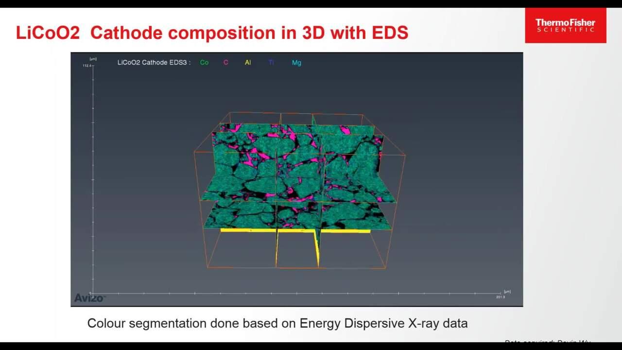
During the slice and view process, both SEM and EDS images are captured every time the focused ion beam exposes a new surface, revealing the elemental composition of that slice. The images are combined to create a 3D map that can be assembled into a video using Thermo Scientific Avizo Software. In this example, the cobalt particles (shown in green) in a lithium cobalt cathode are coated with a layer of titanium (dark blue).
During the battery production process, impurities are always introduced. Impurities such as Fe, Cr, Zn, and Cu particles in battery raw materials have significant impact on the electrochemical performance and material stability and can even cause internal shorts with severe battery safety issues.
Although ICP-OES is widely used as a standard manufacturing QC process to detect impurities, it does not provide information such as their size and composition, which is needed to identify the contaminant source in the materials production environment and help optimize the manufacturing process. The Thermo Scientific Phenom ParticleX Battery Desktop SEM provides an automated SEM-EDS workflow that can identify and quantify impurities in battery materials.
Identified particle contamination in NMC powders
The Phenom ParticleX Battery Desktop SEM was used to identify impurities in NMC powders and populate the final data table with composition and size information. The fully automated workflow helps identify impurities in battery raw materials with high throughput.


| Challenge | Challenge | Solution | Resources |
| Characterize battery structure at different scales, beyond the capacity of a single instrument | CT, SEM, Raman, DualBeam, Avizo, EDS | Correlative workflow allowing multiscale imaging and analysis of battery microstructure | App note: Multiscale image-based control and characterization of lithium-ion batteries |
| App note: Multiscale 3D imaging solutions for Li-ion batteries | |||
| App note: Understand degradation mechanisms in lithium-ion batteries at different scales | |||
| Prepare a large 2D area on the sample surface with high polishing quality for 2D imaging and characterization | DualBeam (Plasma FIB-SEM), EDS | High-throughput automated spin mill with high surface quality | App note: Large area automated sample preparation for batteries |
| Characterize key microstructure properties (like tortuosity) for electrode structure performance correlations | DualBeam, EDS, TOF-SIMS, Avizo | 3D characterization of battery structure
|
Blog post/video: Advancing lithium-ion battery technology with 3D imaging |
| App note: Multiscale image-based control and characterization of lithium-ion batteries | |||
| Characterize beam-sensitive materials like SEI at nanoscale | TEM, EDS, Avizo | Nano- and atomic-scale characterization of energy materials
|
Brochure: Analytical solutions for battery and energy storage technology |
| Webinar: Cryo- and in situ electron microscopy diagnosis-guided design of rechargeable battery materials for better batteries | |||
| Webinar: Advanced characterization methods of electrochemical materials and interphases for better batteries | |||
| Identification and quantification of metal impurities in materials is critical, but neither ICP nor optical microscopy does both | Desktop SEM, EDS | Phenom ParticleX Desktop SEM can identify and quantify particle impurities with high-throughput automated EDS workflow | Webinar: How to certify your NCM powder quality with SEM+EDS |
| Detection of electrode impurities is slow and tedious using normal SEM-to-EDS workflow | ChemiSEM, EDS | Thermo Scientific Axia ChemiSEM integrates SEM with “live EDS” for immediate characterization of electrode impurities | App note: Assessment of contaminants within battery materials via Axia ChemiSEM |
| Identification of impurities for root cause analysis is difficult using CT alone | CT/SDB, EDS, Avizo | A correlative CT/laser PFIB workflow can identify deeply embedded impurities without disassembling the cell | App note: Multiscale 3D imaging solutions for Li-ion batteries |
Abbreviations: Avizo = Avizo Software; CT = Computed tomography; DualBeam = Focused ion beam scanning electron microscopy (FIB-SEM); EDS = Energy-dispersive X-ray spectroscopy; FIB = Focused ion beam; ICP = Inductively coupled plasma; SDB = Small DualBeam; SEI = solid electrolyte interface; SEM = Scanning electron microscopy; TEM = Transmission electron microscopy; TOF-SIMS = Time of flight secondary ion mass spectrometry.


ChemiSEM cross-section image of an electrode active material.

SEM BSE (left) and ChemiSEM EDS (right) images of a Li-NMC cathode sample with Zr contaminant. Captured on the Axia ChemiSEM. Images courtesy of Alice Scarpellini, Thermo Fisher Scientific.

ChemiSEM image of nickel, copper, and zinc particles
Before (left) and after (right) ChemiSEM application at 50 µm magnification.

ChemiSEM image of nickel (cyan) in a Li-ion battery cathode
Characterized with Axia ChemiSEM. Image courtesy of Alice Scarpellini, Thermo Fisher Scientific.

Live tooltip feature on a SiO/C battery anode
The tooltip shows the relative concentrations of the sample constituents—a quick, easy way to obtain composition information during live imaging.
Brochures
Datasheets
For Research Use Only. Not for use in diagnostic procedures.