Search Thermo Fisher Scientific
Thermo Scientific AutoTEM 5 Software is a unique solution for DualBeam (focused ion beam scanning electron microscopy, FIB-SEM) systems, supporting fully automated, in situ transmission electron microscopy (TEM) sample preparation for a wide range of materials science samples. It provides fast, reliable, and repeatable results for users with any experience level.
High quality
High quality S/TEM sample preparation for users of any experience level in less than one hour.
Complete workflow
Complete in situ S/TEM sample preparation workflow, including automated chunking, user guided lift-out and automated final thinning.
Automated in-situ sample preparation
Fully automated in-situ sample preparation using different geometries: top down, plan view and inverted.
Robust results
Robust, predictable results for a wide range of material science samples
High throughput
High throughput with fully automated, unattended multi-site in-situ and ex-situ lift out and auto cross-section capabilities.
Highly configurable workflow
Highly configurable workflow to enable preparation of challenging samples.
Manual preparation | AutoTEM 5 Software | ||
|---|---|---|---|
Materials | Metals and alloys | ||
Semiconductors | |||
Polymers and ceramics | |||
Process coverage | Chunk milling | Manual | Fully automated or interactive |
Lift-out process | Manual | ||
Final thinning | Manual | ||
Low-energy polishing | Manual | ||
Specifications | Throughput | 60 – 120 mins | < 45 mins |
High quality | User dependent | Protocol dependent | |
Repeatability | - | ||
Overnight runs | - | ||
User | Experience level | Expert | Beginner |
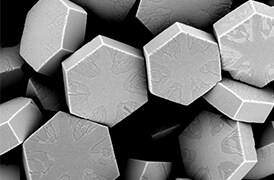
Fundamental Materials Research
Novel materials are investigated at increasingly smaller scales for maximum control of their physical and chemical properties. Electron microscopy provides researchers with key insight into a wide variety of material characteristics at the micro- to nano-scale.
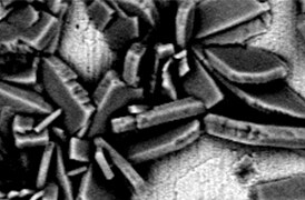
Process control using electron microscopy
Modern industry demands high throughput with superior quality, a balance that is maintained through robust process control. SEM and TEM tools with dedicated automation software provide rapid, multi-scale information for process monitoring and improvement.
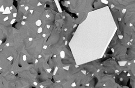
Quality control and failure analysis
Quality control and assurance are essential in modern industry. We offer a range of EM and spectroscopy tools for multi-scale and multi-modal analysis of defects, allowing you to make reliable and informed decisions for process control and improvement.
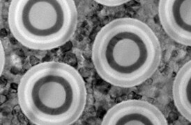
Semiconductor Pathfinding and Research
Advanced electron microscopy, focused ion beam, and associated analytical techniques for identifying viable solutions and design methods for the fabrication of high-performance semiconductor devices.
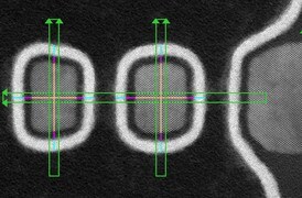
Yield Ramp and Metrology
We offer advanced analytical capabilities for defect analysis, metrology, and process control, designed to help increase productivity and improve yield across a range of semiconductor applications and devices.
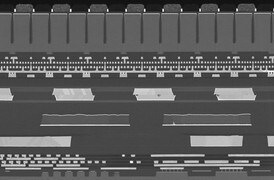
Semiconductor Failure Analysis
Increasingly complex semiconductor device structures result in more places for failure-inducing defects to hide. Our next-generation workflows help you localize and characterize subtle electrical issues that affect yield, performance, and reliability.

Physical and Chemical Characterization
Ongoing consumer demand drives the creation of smaller, faster, and cheaper electronic devices. Their production relies on high-productivity instruments and workflows that image, analyze, and characterize a broad range of semiconductor and display devices.

(S)TEM Sample Preparation
DualBeam microscopes enable the preparation of high-quality, ultra-thin samples for (S)TEM analysis. Thanks to advanced automation, users with any experience level can obtain expert-level results for a wide range of materials.

Cross-sectioning
Cross sectioning provides extra insight by revealing sub-surface information. DualBeam instruments feature superior focused ion beam columns for high-quality cross sectioning. With automation, unattended high-throughput processing of samples is possible.

Multi-scale analysis
Novel materials must be analyzed at ever higher resolution while retaining the larger context of the sample. Multi-scale analysis allows for the correlation of various imaging tools and modalities such as X-ray microCT, DualBeam, Laser PFIB, SEM and TEM.
Semiconductor TEM Imaging and Analysis
Thermo Scientific transmission electron microscopes offer high-resolution imaging and analysis of semiconductor devices, enabling manufacturers to calibrate toolsets, diagnose failure mechanisms, and optimize overall process yields.
TEM Metrology
Advanced and automated TEM metrology routines deliver significantly greater precision than manual methods. This allows users to generate large amounts of statistically relevant data, with sub-angstrom-level specificity, that is free of operator bias.
Sample Preparation of Semiconductor Devices
Thermo Scientific DualBeam systems provide accurate TEM sample preparation for atomic-scale analysis of semiconductor devices. Automation and advanced machine learning technologies produce high-quality samples, at the correct location, and a low cost per sample.
Semiconductor Laser Ablation
Laser ablation provides high-throughput milling of semiconductor devices for imaging and analysis with electron microscopy, while still preserving sample integrity. Access large-volume 3D data and optimize milling conditions to best suit your sample type.

(S)TEM Sample Preparation
DualBeam microscopes enable the preparation of high-quality, ultra-thin samples for (S)TEM analysis. Thanks to advanced automation, users with any experience level can obtain expert-level results for a wide range of materials.

Cross-sectioning
Cross sectioning provides extra insight by revealing sub-surface information. DualBeam instruments feature superior focused ion beam columns for high-quality cross sectioning. With automation, unattended high-throughput processing of samples is possible.

Multi-scale analysis
Novel materials must be analyzed at ever higher resolution while retaining the larger context of the sample. Multi-scale analysis allows for the correlation of various imaging tools and modalities such as X-ray microCT, DualBeam, Laser PFIB, SEM and TEM.
Semiconductor TEM Imaging and Analysis
Thermo Scientific transmission electron microscopes offer high-resolution imaging and analysis of semiconductor devices, enabling manufacturers to calibrate toolsets, diagnose failure mechanisms, and optimize overall process yields.
TEM Metrology
Advanced and automated TEM metrology routines deliver significantly greater precision than manual methods. This allows users to generate large amounts of statistically relevant data, with sub-angstrom-level specificity, that is free of operator bias.
Sample Preparation of Semiconductor Devices
Thermo Scientific DualBeam systems provide accurate TEM sample preparation for atomic-scale analysis of semiconductor devices. Automation and advanced machine learning technologies produce high-quality samples, at the correct location, and a low cost per sample.
Semiconductor Laser Ablation
Laser ablation provides high-throughput milling of semiconductor devices for imaging and analysis with electron microscopy, while still preserving sample integrity. Access large-volume 3D data and optimize milling conditions to best suit your sample type.
Electron microscopy services
To ensure optimal system performance, we provide you access to a world-class network of field service experts, technical support, and certified spare parts.


