Search Thermo Fisher Scientific
The need for a more connected, more autonomous, and smarter world drives innovation in semiconductor and microelectronic devices, which require consistent improvements in performance, energy efficiency, security, cost, and reliability. Focus must also be given to improving time-to-market and time-to-yield. However, shrinking geometries, new materials, and novel 3D architectures make these continual improvements increasingly more challenging. As a result, current 2D metrology and inspection workflows are no longer adequate for device manufacturing. Instead, high-productivity 3D analysis workflows are now essential to the fabrication process.
Overall, these 3D analysis tools and workflows give manufacturers the ability to provide high-productivity characterization of a broad range of devices. This includes equipment for ESD compliance testing, efficient pathfinding, advanced imaging and analysis, layer-by-layer device de-processing, laser ablation, and for maximizing yield in the shortest time possible.
Thermo Fisher Scientific provides the broadest portfolio of high-productivity 3D analysis workflows that accelerate development, maximize yields, and ensure the production of high-quality devices that meet current and future industry demands. Explore the pages below to learn how our applications and workflows can address your specific needs.
40 years of semiconductor analysis innovation
With more than four decades innovating physical and electrical analysis solutions for the electronics industry, Thermo Fisher Scientific is one of the world’s premier providers of ultra-high-resolution tools for imaging and analysis at the nanoscale.

Infographic: 40 years of semiconductor analysis innovation

Semiconductor Device Packaging
Advanced semiconductor device packaging requires new integration approaches and innovation in performance, power efficiency, area, and cost. See how Thermo Scientific failure analysis workflows provide fast, precise, and accurate time-to-data for device packaging development.
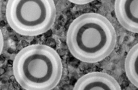
Semiconductor Pathfinding and Research
Advanced electron microscopy, focused ion beam, and associated analytical techniques for identifying viable solutions and design methods for the fabrication of high-performance semiconductor devices.
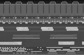
Semiconductor Failure Analysis
Increasingly complex semiconductor device structures result in more places for failure-inducing defects to hide. Our next-generation workflows help you localize and characterize subtle electrical issues that affect yield, performance, and reliability.

Display Module Failure Analysis
Evolving display technologies aim to improve display quality and light conversion efficiency to support applications in different industry sectors, while continuing to reduce production costs. Our process metrology, failure analysis and research and development solutions help display companies solve these challenges.

ESD Semiconductor Qualification
Every electrostatic discharge (ESD) control plan is required to identify devices that are sensitive to ESD. We offer a complete suite of test systems to help with your device qualification requirements.
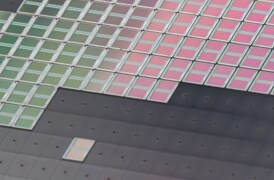
Memory Device Metrology and Analysis
Modern data demands are driving innovation in 3D NAND, DRAM and other memory structures. Our memory analysis tools and workflows offer high-productivity characterization so that manufacturers can meet performance, latency, and capacity demands.
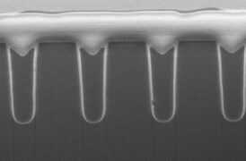
Power Semiconductor Device Analysis
Power devices pose unique challenges for localizing faults, primarily as a result of power device architecture and layout. Our power device analysis tools and workflows quickly pinpoint fault locations at operating conditions and provide precise, high-throughput analysis for characterization of materials, interfaces and device structures.
Yield Ramp and Metrology
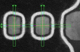
We offer advanced analytical capabilities for defect analysis, metrology, and process control, designed to help increase productivity and improve yield across a range of semiconductor applications and devices.

Physical and Chemical Characterization
Ongoing consumer demand drives the creation of smaller, faster, and cheaper electronic devices. Their production relies on high-productivity instruments and workflows that image, analyze, and characterize a broad range of semiconductor and display devices.
TEM Metrology
Advanced and automated TEM metrology routines deliver significantly greater precision than manual methods. This allows users to generate large amounts of statistically relevant data, with sub-angstrom-level specificity, that is free of operator bias.
Semiconductor TEM Imaging and Analysis
Thermo Scientific transmission electron microscopes offer high-resolution imaging and analysis of semiconductor devices, enabling manufacturers to calibrate toolsets, diagnose failure mechanisms, and optimize overall process yields.
Circuit Edit
Advanced, dedicated circuit edit and nanoprototyping solutions, which combine novel gas-delivery systems with a broad portfolio of chemistries and focused ion beam technology, offer unparalleled control and precision for semiconductor device development.
SEM Metrology
Scanning electron microscopy provides accurate and reliable metrology data at nanometer scales. Automated ultra-high-resolution SEM metrology enables faster time-to-yield and time-to-market for memory, logic, and data storage applications.
Semiconductor Analysis and Imaging
Thermo Fisher Scientific offers scanning electron microscopes for every function of a semiconductor lab, from general imaging tasks to advanced failure analysis techniques requiring precise voltage-contrast measurements.
Optical Fault Isolation
Increasingly complex designs complicate fault and defect isolation in semiconductor manufacturing. Optical fault isolation techniques allow you to analyze the performance of electrically active devices to locate critical defects that cause device failure.
Thermal Fault Isolation
Uneven distribution of local power dissipation can cause large, localized increases in temperature, leading to device failure. We offer unique solutions for thermal fault isolation with high-sensitivity lock-in infrared thermography (LIT).
Sample Preparation of Semiconductor Devices
Thermo Scientific DualBeam systems provide accurate TEM sample preparation for atomic-scale analysis of semiconductor devices. Automation and advanced machine learning technologies produce high-quality samples, at the correct location, and a low cost per sample.
Nanoprobing
As device complexity increases, so does the number of places defects have to hide. Nanoprobing provides the precise localization of electrical faults, which is critical for an effective transmission electron microscopy failure analysis workflow.

APT Sample Preparation
Atom probe tomography (APT) provides atomic-resolution 3D compositional analysis of materials. Focused ion beam (FIB) microscopy is an essential technique for high-quality, orientation, and site-specific sample preparation for APT characterization.
Semiconductor Laser Ablation
Laser ablation provides high-throughput milling of semiconductor devices for imaging and analysis with electron microscopy, while still preserving sample integrity. Access large-volume 3D data and optimize milling conditions to best suit your sample type.
Device Delayering
Shrinking feature size, along with advanced design and architecture, results in increasingly challenging failure analysis for semiconductors. Damage-free delayering of devices is a critical technique for the detection of buried electrical faults and failures.
ESD Compliance Testing
Electrostatic discharge (ESD) can damage small features and structures in semiconductors and integrated circuits. We offer a comprehensive suite of test equipment which verifies that your devices meet targeted ESD compliance standards.
Spectroscopic Solutions
Electronic, photonic and magnetic materials are key drivers in technological advancements for information storage, processing and delivery.
Process Mass Spectrometer
With our APIX δQ and APIX Quattro gas analyzers, you can continuously measure bulk gases with more accurate analysis and lower detection limits than other technologies. Thanks to API-MS, advanced electronics and powerful software backed by our expertise, you now have a smart solution for quality control – protecting wafer production and avoiding significant costs.
TEM Metrology
Advanced and automated TEM metrology routines deliver significantly greater precision than manual methods. This allows users to generate large amounts of statistically relevant data, with sub-angstrom-level specificity, that is free of operator bias.
Semiconductor TEM Imaging and Analysis
Thermo Scientific transmission electron microscopes offer high-resolution imaging and analysis of semiconductor devices, enabling manufacturers to calibrate toolsets, diagnose failure mechanisms, and optimize overall process yields.
Circuit Edit
Advanced, dedicated circuit edit and nanoprototyping solutions, which combine novel gas-delivery systems with a broad portfolio of chemistries and focused ion beam technology, offer unparalleled control and precision for semiconductor device development.
SEM Metrology
Scanning electron microscopy provides accurate and reliable metrology data at nanometer scales. Automated ultra-high-resolution SEM metrology enables faster time-to-yield and time-to-market for memory, logic, and data storage applications.
Semiconductor Analysis and Imaging
Thermo Fisher Scientific offers scanning electron microscopes for every function of a semiconductor lab, from general imaging tasks to advanced failure analysis techniques requiring precise voltage-contrast measurements.
Optical Fault Isolation
Increasingly complex designs complicate fault and defect isolation in semiconductor manufacturing. Optical fault isolation techniques allow you to analyze the performance of electrically active devices to locate critical defects that cause device failure.
Thermal Fault Isolation
Uneven distribution of local power dissipation can cause large, localized increases in temperature, leading to device failure. We offer unique solutions for thermal fault isolation with high-sensitivity lock-in infrared thermography (LIT).
Sample Preparation of Semiconductor Devices
Thermo Scientific DualBeam systems provide accurate TEM sample preparation for atomic-scale analysis of semiconductor devices. Automation and advanced machine learning technologies produce high-quality samples, at the correct location, and a low cost per sample.
Nanoprobing
As device complexity increases, so does the number of places defects have to hide. Nanoprobing provides the precise localization of electrical faults, which is critical for an effective transmission electron microscopy failure analysis workflow.

APT Sample Preparation
Atom probe tomography (APT) provides atomic-resolution 3D compositional analysis of materials. Focused ion beam (FIB) microscopy is an essential technique for high-quality, orientation, and site-specific sample preparation for APT characterization.
Semiconductor Laser Ablation
Laser ablation provides high-throughput milling of semiconductor devices for imaging and analysis with electron microscopy, while still preserving sample integrity. Access large-volume 3D data and optimize milling conditions to best suit your sample type.
Device Delayering
Shrinking feature size, along with advanced design and architecture, results in increasingly challenging failure analysis for semiconductors. Damage-free delayering of devices is a critical technique for the detection of buried electrical faults and failures.
ESD Compliance Testing
Electrostatic discharge (ESD) can damage small features and structures in semiconductors and integrated circuits. We offer a comprehensive suite of test equipment which verifies that your devices meet targeted ESD compliance standards.
Spectroscopic Solutions
Electronic, photonic and magnetic materials are key drivers in technological advancements for information storage, processing and delivery.
Process Mass Spectrometer
With our APIX δQ and APIX Quattro gas analyzers, you can continuously measure bulk gases with more accurate analysis and lower detection limits than other technologies. Thanks to API-MS, advanced electronics and powerful software backed by our expertise, you now have a smart solution for quality control – protecting wafer production and avoiding significant costs.
Documents
Semiconductor Overview Brochure ›
Semiconductor Solutions Brochure ›
Spec Sheet: APIX δQ and APIX Quattro ›
Infographic: 5 reasons to use ultra high purity gas analyzers in the semiconductor industry ›
eBook: Gain process understanding and control ›
Characterization of Amorphous and Microcrystalline Silicon using Raman Spectroscopy Brochure ›
Analysis of Hazardous Substances and Products for WEEE/RoHS Compliance Brochure ›
App & Tech Notes
Application Note: Determination of Trace Anions in High Purity Waters using a Large-Volume Direct Injection ›
Application Note: Trace Borate Determination in High-Purity Waters ›
Application Note: Determination of Additives and Byproducts in an Acid Copper Plating Bath by Liquid Chromatography ›
Application Note: Thermo Scientific™ APIX δQ and APIX Quattro Process Mass Spectrometers ›
Application Note: Quantitative Determination of Hydrogen Concentration in Silicon Nitride Dielectric Films on Silicon Wafers using FTIR Spectroscopy ›
Application Note: Analysis of TFT Glass with ARL PERFORM'X WDXRF Spectrometer ›
Application Note: Application Note: Investigation of Ni on Si Thin Film with ARL EQUINOX 100 X-ray Diffractometer ›
Application Note: Analysis of Copper Indium Gallium Selenide (CIGS) Solar Cells with EDXRF ›
Technical Note: Techniques for Successful Trace Anion and Trace Cation Determinations in High Purity Waters ›
Blog
Accelerating Microscopy Blog ›
Advancing Mining Blog ›
Analyzing Metals Blog ›
Analyte Guru Blog ›
Advancing Materials Blog ›
Ultra-High Purity (UHP) Electronic Gas Analyzers in Semiconductor Industry ›
Evaluating Ceramic Materials for 5G Networks ›
Fabricating and Characterizing Thin Film Materials ›
SEM: Types of Electrons and the Information They Provide ›
Platinum Group Metals Connect: Electronics Applications ›
More Information
Image Gallery for Electron Microscopy ›
Semiconductor Analysis, Imaging, and Metrology Information ›
Plating Baths Information ›
Batteries & Capacitors Information ›
Microelectronics Information ›
Materials Science Research ›
Food Solutions Through Rheology & Extrusion ›
Ultra-High Purity Electronic Gas Analyzer in the Semiconductor Industry ›
Semiconductor Materials and Device Characterization
As semiconductor devices shrink and become more complex, new designs and structures are needed. High-productivity 3D analysis workflows can shorten device development time, maximize yield, and ensure that devices meet the future needs of the industry.
Lab Instrument & Equipment Services
We offer an unmatched combination of innovative technologies, comprehensive services and unsurpassed technical support. And we are dedicated to keeping your precision lab instruments tuned, qualified, and running flawlessly.
Unity Lab Services
Unity Lab Services offers specialized, end-to-end services that enable scientists to maximize operational productivity through our network of world-class service and support personnel. As lab service and support experts and partners, the Unity Lab Services team provides training, equipment servicing and asset management, as well as dedicated supply management.
Instrument Product Support
Get help with instrument support, field service fulfillment, and depot repair.
Electron microscopy services for
semiconductors
To ensure optimal system performance, we provide you access to a world-class network of field service experts, technical support, and certified spare parts.


