Search Thermo Fisher Scientific
3D tomography software
Thermo Scientific Inspect 3D Software provides a user-friendly solution for alignment of tomographic image series (obtained with transmission electron microscopy or scanning transmission electron microscopy, TEM or STEM) along with energy dispersive X-ray spectroscopy (EDS) maps, producing a 3D reconstruction of the data. Inspect 3D Software also offers basic visualization functionality. All Thermo Scientific TEM, STEM and EDS tomography software are fully compatible with Inspects 3D Software.
Inspect 3D Software begins with a coarse X-Y alignment based on image cross-correlation. Alignment can be further refined with automated bead tracking or patch tracking procedures. Bead tracking traces multiple round particles on the specimen throughout the tilt series, correcting rotation and magnification changes for each image. Patch tracking traces multiple areas of the image throughout the tilt series and then combines the results.
Inspect 3D Software offers two classical algorithms for 3D volume reconstruction: weighted back projection (WBP) and simultaneous iterative reconstruction technique (SIRT). Additionally, Inspect 3D Software offers easy EDS-tomography reconstruction with simultaneous processing of STEM and EDS files, called HAADF-EDS bimodal tomography (HEBT), leading to enhanced elemental reconstruction.
Iterative reconstruction techniques offered with Inspect 3D Software include;
- Conjugate gradient least squares (CGLS)
- Expectation maximization (EM), in which elongation artifacts are significantly reduced when compared to SIRT reconstruction
- Simultaneous algebraic reconstruction technique (SART)
The resulting reconstructed volumes can be directly imported into Thermo Scientific Avizo and Amira Software for further visualization and analysis.
- Cross-correlation requires no markers as the process is enhanced by the use of a large variety of filters and image processing tools.
- Feature tracking can utilize added artificial features like gold markers, or recognizable intrinsic specimen features, as a basis for image alignment.
- Bead cloaking removes gold beads from the image data after they have been used for alignment, so they do not show in the reconstruction.
- The algebraic reconstruction technique iteratively compares projections of the reconstruction to the original projections and corrects the reconstruction to minimize differences.
- The simultaneous iterative reconstruction technique preserves full spatial information and can enhance the signal to noise ratio of the reconstruction.


Infectious Disease Research
Cryo-EM techniques enable multiscale observations of 3D biological structures in their near-native states, informing faster, more efficient development of therapeutics.
Plant Biology Research
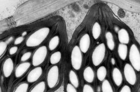
Fundamental plant biology research is enabled by cryo electron microscopy, which provides information on proteins (with single particle analysis), to their cellular context (with tomography), all the way up to the overall structure of the plant (large volume analysis).

Pathology Research
Transmission electron microscopy (TEM) is used when the nature of the disease cannot be established via alternative methods. With nano-biological imaging, TEM provides accurate and reliable insight for certain pathologies.
Process control using electron microscopy
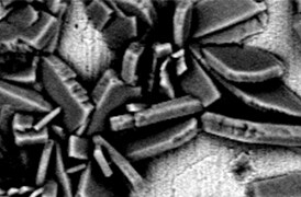
Modern industry demands high throughput with superior quality, a balance that is maintained through robust process control. SEM and TEM tools with dedicated automation software provide rapid, multi-scale information for process monitoring and improvement.
Quality control and failure analysis
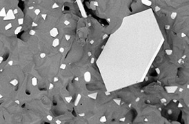
Quality control and assurance are essential in modern industry. We offer a range of EM and spectroscopy tools for multi-scale and multi-modal analysis of defects, allowing you to make reliable and informed decisions for process control and improvement.
Fundamental Materials Research
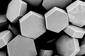
Novel materials are investigated at increasingly smaller scales for maximum control of their physical and chemical properties. Electron microscopy provides researchers with key insight into a wide variety of material characteristics at the micro- to nano-scale.
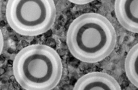
Semiconductor Pathfinding and Research
Advanced electron microscopy, focused ion beam, and associated analytical techniques for identifying viable solutions and design methods for the fabrication of high-performance semiconductor devices.
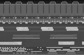
Semiconductor Failure Analysis
Increasingly complex semiconductor device structures result in more places for failure-inducing defects to hide. Our next-generation workflows help you localize and characterize subtle electrical issues that affect yield, performance, and reliability.

Physical and Chemical Characterization
Ongoing consumer demand drives the creation of smaller, faster, and cheaper electronic devices. Their production relies on high-productivity instruments and workflows that image, analyze, and characterize a broad range of semiconductor and display devices.

Single Particle Analysis
Single particle analysis (SPA) is a cryo-electron microscopy technique that enables structural characterization at near-atomic resolutions, unraveling dynamic biological processes and the structure of biomolecular complexes/assemblies.

Cryo-Tomography
Cryo-electron tomography (cryo-ET) delivers both structural information about individual proteins as well as their spatial arrangements within the cell. This makes it a truly unique technique and also explains why the method has such an enormous potential for cell biology. Cryo-ET can bridge the gap between light microscopy and near-atomic-resolution techniques like single-particle analysis.

3D Materials Characterization
Development of materials often requires multi-scale 3D characterization. DualBeam instruments enable serial sectioning of large volumes and subsequent SEM imaging at nanometer scale, which can be processed into high-quality 3D reconstructions of the sample.
_Technique_800x375_144DPI.jpg)
3D EDS Tomography
Modern materials research is increasingly reliant on nanoscale analysis in three dimensions. 3D characterization, including compositional data for full chemical and structural context, is possible with 3D EM and energy dispersive X-ray spectroscopy.
Semiconductor TEM Imaging and Analysis
Thermo Scientific transmission electron microscopes offer high-resolution imaging and analysis of semiconductor devices, enabling manufacturers to calibrate toolsets, diagnose failure mechanisms, and optimize overall process yields.

Single Particle Analysis
Single particle analysis (SPA) is a cryo-electron microscopy technique that enables structural characterization at near-atomic resolutions, unraveling dynamic biological processes and the structure of biomolecular complexes/assemblies.

Cryo-Tomography
Cryo-electron tomography (cryo-ET) delivers both structural information about individual proteins as well as their spatial arrangements within the cell. This makes it a truly unique technique and also explains why the method has such an enormous potential for cell biology. Cryo-ET can bridge the gap between light microscopy and near-atomic-resolution techniques like single-particle analysis.

3D Materials Characterization
Development of materials often requires multi-scale 3D characterization. DualBeam instruments enable serial sectioning of large volumes and subsequent SEM imaging at nanometer scale, which can be processed into high-quality 3D reconstructions of the sample.
_Technique_800x375_144DPI.jpg)
3D EDS Tomography
Modern materials research is increasingly reliant on nanoscale analysis in three dimensions. 3D characterization, including compositional data for full chemical and structural context, is possible with 3D EM and energy dispersive X-ray spectroscopy.
Semiconductor TEM Imaging and Analysis
Thermo Scientific transmission electron microscopes offer high-resolution imaging and analysis of semiconductor devices, enabling manufacturers to calibrate toolsets, diagnose failure mechanisms, and optimize overall process yields.
Electron microscopy services
To ensure optimal system performance, we provide you access to a world-class network of field service experts, technical support, and certified spare parts.
