48ab - Appl/Samples/Products/Resources/Contact

Energy-dispersive X-ray spectroscopy

Energy-dispersive X-ray spectroscopy (EDS, also abbreviated EDX or XEDS) is an analytical technique that enables the chemical characterization/elemental analysis of materials. A sample excited by an energy source (such as the electron beam of an electron microscope) dissipates some of the absorbed energy by ejecting a core-shell electron. A higher energy outer-shell electron then proceeds to fill its place, releasing the difference in energy as an X-ray that has a characteristic spectrum based on its atom of origin. This allows for the compositional analysis of a given sample volume that has been excited by the energy source. The position of the peaks in the spectrum identifies the element, whereas the intensity of the signal corresponds to the concentration of the element.

EDS elemental mapping

As previously stated, an electron beam provides sufficient energy to eject core-shell electrons and cause X-ray emission. Compositional information, down to the atomic level, can be obtained with the addition of an EDS detector to an electron microscope. As the electron probe is scanned across the sample, characteristic X-rays are emitted and measured; each recorded EDS spectrum is mapped to a specific position on the sample. The quality of the results depends on the signal strength and the cleanliness of the spectrum. Signal strength relies heavily on a good signal-to-noise ratio, particularly for trace element detection and dose minimization (which allows for faster recording and artifact-free results). Cleanliness will impact the number of spurious peaks seen; this is a consequence of the materials that make up the electron column.

EDS materials analysis

  • Sensitive to low concentrations—minimum detection limits below 0.1% in the best cases
  • Affords a high degree of relative precision—typically 2–4%
  • Non-destructive in most situations
  • Usually requires minimal sample preparation effort and time
  • Delivers complete analyses of complex samples quickly, often in under a minute

Advanced and fully integrated EDS solutions are available on Thermo Scientific TEM, SEM and Desktop systems.

Elemental mapping software


Resources

Segmented surface rendering of nanoparticles colored with elements present: silver cores (red) with platinum shells (green). To increase visibility, the platinum shells have been colored semitransparent. Sample Courtesy of Prof. Yi Ding and Prof. Jun Luo, Center for Electron Microscopy, Tianjin University of Technology.

EDS tomography of P-Zn-In nanotubes. Sample courtesy of Dr. Reza Shahbazian Yassar, Michigan Tech University.

Applications

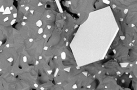
Aluminum mineral grain found with SEM during parts cleanliness testing

Technical Cleanliness

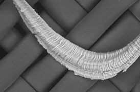
More than ever, modern manufacturing necessitates reliable, quality components. With scanning electron microscopy, parts cleanliness analysis can be brought inhouse, providing you with a broad range of analytical data and shortening your production cycle.
Quality control and failure analysis using electron microscopy

Quality control and failure analysis

Quality control and assurance are essential in modern industry. We offer a range of EM and spectroscopy tools for multi-scale and multi-modal analysis of defects, allowing you to make reliable and informed decisions for process control and improvement.
Fundamental Materials Research_R&D_Thumb_274x180_144DPI

Fundamental Materials Research

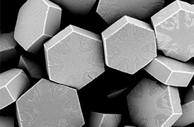
Novel materials are investigated at increasingly smaller scales for maximum control of their physical and chemical properties. Electron microscopy provides researchers with key insight into a wide variety of material characteristics at the micro- to nano-scale.


Samples


Battery Research

Battery development is enabled by multi-scale analysis with microCT, SEM and TEM, Raman spectroscopy, XPS, and digital 3D visualization and analysis. Learn how this approach provides the structural and chemical information needed to build better batteries.

Learn more ›


Polymers Research

Polymer microstructure dictates the material’s bulk characteristics and performance. Electron microscopy enables comprehensive microscale analysis of polymer morphology and composition for R&D and quality control applications.

Learn more ›


Metals Research

Effective production of metals requires precise control of inclusions and precipitates. Our automated tools can perform a variety of tasks critical for metal analysis including; nanoparticle counting, EDS chemical analysis and TEM sample preparation.

Learn more ›


Oil and Gas

As the demand for oil and gas continues, there is an ongoing need for efficient and effective extraction of hydrocarbons. Thermo Fisher Scientific offers a range of microscopy and spectroscopy solutions for a variety of petroleum science applications.

Learn more ›


Nanoparticles

Materials have fundamentally different properties at the nanoscale than at the macroscale. To study them, S/TEM instrumentation can be combined with energy dispersive X-ray spectroscopy to obtain nanometer, or even sub-nanometer, resolution data.

Learn more ›


Geological Research

Geoscience relies on consistent and accurate multi-scale observation of features within rock samples. SEM-EDS, combined with automation software, enables direct, large-scale analysis of texture and mineral composition for petrology and mineralogy research.

Learn more ›


Forensics

Micro-traces of crime scene evidence can be analyzed and compared using electron microscopy as part of a forensic investigation. Compatible samples include glass and paint fragments, tool marks, drugs, explosives, and GSR (gunshot residue).

Learn more ›


2D Materials

Novel materials research is increasingly interested in the structure of low-dimensional materials. Scanning transmission electron microscopy with probe correction and monochromation allows for high-resolution two-dimensional materials imaging.

Learn more ›


Catalysis Research

Catalysts are critical for a majority of modern industrial processes. Their efficiency depends on the microscopic composition and morphology of the catalytic particles; EM with EDS is ideally suited for studying these properties.

Learn more ›


Automotive Materials Testing

Every component in a modern vehicle is designed for safety, efficiency, and performance. Detailed characterization of automotive materials with electron microscopy and spectroscopy informs critical process decisions, product improvements, and new materials.

Learn more ›


Products

Style Sheet for Instrument Cards Original

Spectra Ultra

  • New imaging and spectroscopy capabilities on the most beam sensitive materials
  • A leap forward in EDX detection with Ultra-X
  • Column designed to maintain sample integrity.

Spectra 200

  • High-resolution and contrast imaging for accelerating voltages from 30-200 kV
  • Symmetric S-TWIN/X-TWIN objective lens with wide-gap pole piece design of 5.4 mm
  • Sub-Angstrom STEM imaging resolution from 60 kV-200 kV

Spectra 300

  • Highest-resolution structural and chemical information at the atomic level
  • Flexible high-tension range from 30-300 kV
  • Three lens condenser system
Thermo Scientific Talos L120C transmission electron microscope (TEM)

Talos L120C TEM

  • Increased stability
  • 4k × 4K Ceta CMOS camera
  • TEM magnification range from 25–650 kX
  • Flexible EDS analysis reveals chemical information

Talos F200i TEM

  • High-quality, high-resolution (S)TEM imaging and flexible EDS
  • Available with high-resolution, high-brightness (cold) field emission guns
  • Available with Dual EDS for highest analytical throughput

Talos F200X TEM

  • High-quality, high-resolution (S)TEM imaging and accurate EDS
  • Available with high-resolution, high-brightness (cold) field emission gun
  • Available with in-column Super-X G2 EDS with ultimate cleanliness
Thermo Scientific Talos F200C transmission electron microscope (TEM)

Talos F200C TEM

  • Flexible EDS analysis reveals chemical information
  • High-contrast, high-quality TEM and STEM imaging
  • Ceta 16 Mpixel CMOS camera provides large field of view and high read-out speed

Talos F200S TEM

  • Precise chemical composition data
  • High-performance imaging and precise compositional analysis for dynamic microscopy
  • Features Velox Software for fast and easy acquisition and analysis of multimodal data
Thermo Scientific Helios Hydra plasma focused ion beam scanning electron microscope (DualBeam)

Helios Hydra DualBeam

  • 4 fast switchable ion species (Xe, Ar, O, N) for optimized PFIB processing of a widest range of materials
  • Ga-free TEM sample preparation
  • Extreme high resolution SEM imaging

Helios 5 PFIB DualBeam

  • Gallium-free STEM and TEM sample preparation
  • Multi-modal subsurface and 3D information
  • Next-generation 2.5 μA xenon plasma FIB column

Helios 5 DualBeam

  • Fully automated, high-quality, ultra-thin TEM sample preparation
  • High throughput, high resolution subsurface and 3D characterization
  • Rapid nanoprototyping capabilities
Thermo Scientific Verios 5 XHR scanning electron microscope (SEM)

Verios 5 XHR SEM

  • Monochromated SEM for sub-nanometer resolution over the full 1 keV to 30 keV energy range
  • Easy access to beam landing energies as low as 20 eV
  • Excellent stability with piezo stage as standard
Thermo Scientific Quattro E scanning electron microscope (SEM)

Quattro ESEM

  • Ultra-versatile high-resolution FEG SEM with unique environmental capability (ESEM)
  • Observe all information from all samples with simultaneous SE and BSE imaging in every mode of operation
Thermo Scientific Prisma E scanning electron microscope (SEM)

Prisma E SEM

  • Entry-level SEM with excellent image quality
  • Easy and quick sample loading and navigation for multiple samples
  • Compatible with a wide range of materials thanks to dedicated vacuum modes

VolumeScope 2 SEM

  • Isotropic 3D data from large volumes
  • High contrast and resolution in high and low vacuum modes
  • Simple switch between normal SEM use and serial block-face imaging
Thermo Scientific Apreo 2 scanning electron microscope (SEM)

Apreo 2 SEM

  • High-performance SEM for all-round nanometer or sub-nanometer resolution
  • In-column T1 backscatter detector for sensitive, TV-rate materials contrast
  • Excellent performance at long working distance (10 mm)
Thermo Scientific Scios 2 plasma focused ion beam scanning electron microscope (DualBeam)

Scios 2 DualBeam

  • Full support of magnetic and non-conductive samples
  • High throughput subsurface and 3D characterization
  • Advanced ease of use and automation capabilities

Phenom XL G2 Desktop SEM

  • For large samples (100x100 mm) and ideal for automation
  • <10 nm resolution and up to 200,000x magnification; 4.8 kV up to 20 kV acceleration voltage
  • Optional fully integrated EDS and BSE detector

Phenom ProX G6 Desktop SEM

  • High performance desktop SEM with integrated EDS detector
  • Resolution <6 nm (SE) and <8 nm (BSE); magnification up to 350,000x
  • Optional SE detector

Phenom Pro G6 Desktop SEM

  • High performance desktop SEM
  • Resolution <6 nm (SE) and <8 nm (BSE); magnification up to 350,000x
  • Optional SE detector

Phenom ParticleX AM Desktop SEM

  • Versatile desktop SEM with automation software for Additive Manufacturing
  • Resolution <10 nm; magnification up to 200,000x
  • Optional SE detector

Phenom ParticleX TC Desktop SEM

  • Versatile desktop SEM with automation software for Technical Cleanliness
  • Resolution <10 nm; magnification up to 200,000x
  • Optional SE detector

Phenom Pure G6 Desktop SEM

  • Entry level desktop SEM
  • Resolution <15 nm; magnification up to 175,000x
  • Longlife CeB6 source

Phenom Perception GSR Desktop SEM

  • Dedicated automated GSR desktop SEM
  • Resolution <10 nm; magnification up to 200,000x
  • Longlife CeB6 source

Phenom Pharos G2 Desktop FEG-SEM

  • FEG source with 1 – 20 kV acceleration voltage range
  • <2.0 nm (SE) and 3.0 nm (BSE) resolution @ 20 kV
  • Optional fully integrated EDS and SE detector

AsbestoMetric

  • Automated tool for image acquisition, fiber detection and reporting
  • Assisted EDS analysis with fiber revisiting
  • ISO standard report on asbestos analysis

Avizo Software
Materials Science

  • Support for multi-data/multi-view, multi-channel, time series, very large data
  • Advanced multi-mode 2D/3D automatic registration
  • Artifact reduction algorithms
Thermo Scientific Inspect 3D tomography software

Inspect 3D Software

  • Image processing tools and filters for cross-correlation
  • Feature tracking for image alignment
  • Algebraic reconstruction technique for iterative projection comparison
Thermo Scientific Maps electron microscopy software

Maps Software

  • Acquire high-resolution images over large areas
  • Easily find regions of interest
  • Automate image acquisition process
  • Correlate data from different sources

Elemental Mapping

  • Fast and reliable information on the distribution of elements within the sample or the selected line
  • Easily exported and reported results

3D Reconstruction

  • Intuitive user interface, maximum employability
  • Intuitive fully automated user interface
  • Based on 'shape from shading' technology, no stage tilt required

Velox

  • An experiments panel on the left side of the processing window.
  • Live quantitative mapping
  • Interactive detector layout interface for reproducible experiment control and setup
Style Sheet for Komodo Tabs
Style Sheet to change H2 style to p with em-h2-header class

Contact us

Style Sheet for Support and Service footer
Style Sheet for Fonts
Style Sheet for Cards

Electron microscopy services for
the materials science

To ensure optimal system performance, we provide you access to a world-class network of field service experts, technical support, and certified spare parts.