Search Thermo Fisher Scientific

Transmission Electron Microscopes
Metrios AX TEM
High productivity transmission electron microscope for semiconductor metrology and process characterization.
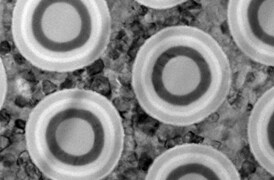
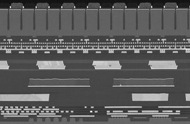
Advanced logic and memory manufacturing processes are becoming more reliant on fast turnaround of precise structural and analytical data to be able to quickly calibrate tool sets, diagnose yield excursions, and optimize process yields. At technology nodes below 28nm, especially in cases where 3D and advanced device designs are being implemented, conventional SEM or optical-based analysis and inspection tools run into challenges that limit their ability to provide robust and reliable data. The Thermo Scientific Metrios AX transmission electron microscope (TEM) is the first TEM dedicated to providing the fast, precise characterization and reference metrology that semiconductor manufacturers need to develop and control their wafer fabrication processes in order to accelerate profitable yield.
High-volume TEM data, accurate and repeatable
The Metrios AX TEM automates the basic TEM operation and measurement procedures, minimizing the requirements for specialized operator training. Its advanced automated metrology routines deliver significantly greater precision than manual methods. The Metrios AX TEM is designed to provide improved throughput and lower cost-per-sample than other TEMs.
Consistent, repeatable, precise
Designed from the ground-up to deliver repeatable TEM and STEM-based imaging, analytics and gauge capable metrology.
Metrology accuracy
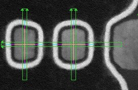
Less than 0.75% combined error in distortion and magnification calibration for both TEM and STEM.
Automated EDS and hybrid metrology
Acquire and quantify EDS data with automation. Use elemental contrast on key critical dimensions to extend STEM.
Workflow connectivity
Critical process data is tracked through sample prep, plucking, and imaging. Metrology can be applied offline to maximize tool acquisition time. All imaging and metrology data is consolidated in a web-based image viewer.
High Tension Range (kV) | 60-200 kV | |
Information Limit 200 kV (nm) | 0.11 | |
Non-corrected | Probe corrected* | |
STEM HAADF Resolution (nm) 200 kV |
|
|
STEM HAADF Resolution (nm) 80 kV |
|
|
Metrology precision on MetroCal wafer for horizontal and vertical |
| |
Electron source |
| |
Ultra-stable electronics and high tension |
| |
Acoustic enclosure |
| |
Constant power lenses |
| |
Piezo stage |
| |
Probe corrector compatible |
| |

Semiconductor Device Packaging
Advanced semiconductor device packaging requires new integration approaches and innovation in performance, power efficiency, area, and cost. See how Thermo Scientific failure analysis workflows provide fast, precise, and accurate time-to-data for device packaging development.

Semiconductor Pathfinding and Research
Advanced electron microscopy, focused ion beam, and associated analytical techniques for identifying viable solutions and design methods for the fabrication of high-performance semiconductor devices.

Yield Ramp and Metrology
We offer advanced analytical capabilities for defect analysis, metrology, and process control, designed to help increase productivity and improve yield across a range of semiconductor applications and devices.

Semiconductor Failure Analysis
Increasingly complex semiconductor device structures result in more places for failure-inducing defects to hide. Our next-generation workflows help you localize and characterize subtle electrical issues that affect yield, performance, and reliability.

Physical and Chemical Characterization
Ongoing consumer demand drives the creation of smaller, faster, and cheaper electronic devices. Their production relies on high-productivity instruments and workflows that image, analyze, and characterize a broad range of semiconductor and display devices.
Semiconductor TEM Imaging and Analysis
Thermo Scientific transmission electron microscopes offer high-resolution imaging and analysis of semiconductor devices, enabling manufacturers to calibrate toolsets, diagnose failure mechanisms, and optimize overall process yields.
TEM Metrology
Advanced and automated TEM metrology routines deliver significantly greater precision than manual methods. This allows users to generate large amounts of statistically relevant data, with sub-angstrom-level specificity, that is free of operator bias.
Electron microscopy services for
semiconductors
To ensure optimal system performance, we provide you access to a world-class network of field service experts, technical support, and certified spare parts.
