Search Thermo Fisher Scientific
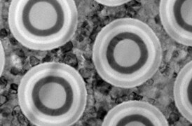
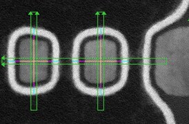
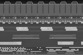
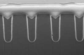
Scanning electron microscopy (SEM) provides high-quality surface and cross-sectional imaging of 3D structures. As semiconductor feature sizes continue to decrease in response to consumer and industry demands, nanoscale metrology becomes an increasingly important contributor to process and device design yield. Accurate and repeatable nanoscale measurements of critical dimensions require high-resolution SEM imaging and extremely accurate magnification calibration.
The ultra-high-resolution automated SEM capabilities offered by Thermo Fisher Scientific, when combined with our industry-leading software solutions, perform imaging and metrology with the automation, precision, and robustness needed to meet the challenges of leading memory and logic customers. Leveraging NIST-traceable calibration standards, mature imaging automation (both cross-sectional and top-down), and next-generation machine-learning-enabled metrology, Thermo Scientific automated SEMs provide cost-effective 3D metrology for direct process and device monitoring, as well as faster time to market.
Thermo Fisher Scientific offers a range of SEM metrology tools for critical dimension analysis, including the Thermo Scientific Verios 5 SEM with Thermo Scientific AutoSEM Software for top-down SEM metrology. Please click through to the appropriate product pages below for more information, or to request a demo.


Semiconductor Pathfinding and Research
Advanced electron microscopy, focused ion beam, and associated analytical techniques for identifying viable solutions and design methods for the fabrication of high-performance semiconductor devices.

Physical and Chemical Characterization
Ongoing consumer demand drives the creation of smaller, faster, and cheaper electronic devices. Their production relies on high-productivity instruments and workflows that image, analyze, and characterize a broad range of semiconductor and display devices.

Yield Ramp and Metrology
We offer advanced analytical capabilities for defect analysis, metrology, and process control, designed to help increase productivity and improve yield across a range of semiconductor applications and devices.

Semiconductor Failure Analysis
Increasingly complex semiconductor device structures result in more places for failure-inducing defects to hide. Our next-generation workflows help you localize and characterize subtle electrical issues that affect yield, performance, and reliability.

Power Semiconductor Device Analysis
Power devices pose unique challenges for localizing faults, primarily as a result of power device architecture and layout. Our power device analysis tools and workflows quickly pinpoint fault locations at operating conditions and provide precise, high-throughput analysis for characterization of materials, interfaces and device structures.

Display Module Failure Analysis
Evolving display technologies aim to improve display quality and light conversion efficiency to support applications in different industry sectors, while continuing to reduce production costs. Our process metrology, failure analysis and research and development solutions help display companies solve these challenges.
Semiconductor Materials and Device Characterization
As semiconductor devices shrink and become more complex, new designs and structures are needed. High-productivity 3D analysis workflows can shorten device development time, maximize yield, and ensure that devices meet the future needs of the industry.
Electron microscopy services for
semiconductors
To ensure optimal system performance, we provide you access to a world-class network of field service experts, technical support, and certified spare parts.


