Search Thermo Fisher Scientific
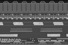
The data demands of artificial intelligence, connected cars, IoT, mobile devices and numerous other applications are driving innovation in memory structures. 3D NAND, DRAM and other advanced memory structures are packing more bits into tighter spaces with higher aspect ratios to meet performance, latency, and capacity demands. With increases in vertical stacking and scaling to smaller cell designs, process complexity, cost, and time-to-market become the greatest challenges affecting manufacturing ramps and profitability.
Challenges in advanced memory technology development
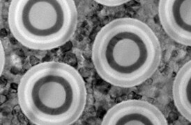
Some of the challenges in 3D NAND development include channel hole and word line profile variability and defectivity, as well as shorts connecting the contacts to the staircase. Challenges in DRAM include storage node capacitor profile variability and defectivity, bit line defects and shrinking multi-patterning overlay error budgets. These process challenges have made current metrology and inspection workflows inadequate. Solving the process issues in these complex stacks requires new tools and workflows that achieve faster time to yield during the development phase and sustain it for high-volume manufacturing.
Memory analysis tools and workflows
Memory analysis tools and workflows must provide manufacturers with high-productivity characterization of a broad range of memory devices to maximize yield in the shortest time possible. This includes equipment for layer-by-layer through-stack metrology, advanced imaging and analysis, automated device de-processing, efficient pathfinding, and ESD compliance testing.
Thermo Fisher Scientific provides the broadest portfolio of high-productivity memory analysis workflows that accelerate development, maximize yields, and ensure the production of high-quality devices that meet current and future industry demands. Explore the pages below to learn how our applications and workflows can address your specific needs.

Semiconductor Pathfinding and Research
Advanced electron microscopy, focused ion beam, and associated analytical techniques for identifying viable solutions and design methods for the fabrication of high-performance semiconductor devices.

Yield Ramp and Metrology
We offer advanced analytical capabilities for defect analysis, metrology, and process control, designed to help increase productivity and improve yield across a range of semiconductor applications and devices.

Semiconductor Failure Analysis
Increasingly complex semiconductor device structures result in more places for failure-inducing defects to hide. Our next-generation workflows help you localize and characterize subtle electrical issues that affect yield, performance, and reliability.

Physical and Chemical Characterization
Ongoing consumer demand drives the creation of smaller, faster, and cheaper electronic devices. Their production relies on high-productivity instruments and workflows that image, analyze, and characterize a broad range of semiconductor and display devices.

ESD Semiconductor Qualification
Every electrostatic discharge (ESD) control plan is required to identify devices that are sensitive to ESD. We offer a complete suite of test systems to help with your device qualification requirements.
Nanoprobing
As device complexity increases, so does the number of places defects have to hide. Nanoprobing provides the precise localization of electrical faults, which is critical for an effective transmission electron microscopy failure analysis workflow.
Optical Fault Isolation
Increasingly complex designs complicate fault and defect isolation in semiconductor manufacturing. Optical fault isolation techniques allow you to analyze the performance of electrically active devices to locate critical defects that cause device failure.
Thermal Fault Isolation
Uneven distribution of local power dissipation can cause large, localized increases in temperature, leading to device failure. We offer unique solutions for thermal fault isolation with high-sensitivity lock-in infrared thermography (LIT).
Semiconductor TEM Imaging and Analysis
Thermo Scientific transmission electron microscopes offer high-resolution imaging and analysis of semiconductor devices, enabling manufacturers to calibrate toolsets, diagnose failure mechanisms, and optimize overall process yields.
TEM Metrology
Advanced and automated TEM metrology routines deliver significantly greater precision than manual methods. This allows users to generate large amounts of statistically relevant data, with sub-angstrom-level specificity, that is free of operator bias.
Sample Preparation of Semiconductor Devices
Thermo Scientific DualBeam systems provide accurate TEM sample preparation for atomic-scale analysis of semiconductor devices. Automation and advanced machine learning technologies produce high-quality samples, at the correct location, and a low cost per sample.
SEM Metrology
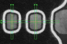
Scanning electron microscopy provides accurate and reliable metrology data at nanometer scales. Automated ultra-high-resolution SEM metrology enables faster time-to-yield and time-to-market for memory, logic, and data storage applications.
Semiconductor Analysis and Imaging
Thermo Fisher Scientific offers scanning electron microscopes for every function of a semiconductor lab, from general imaging tasks to advanced failure analysis techniques requiring precise voltage-contrast measurements.
Device Delayering
Shrinking feature size, along with advanced design and architecture, results in increasingly challenging failure analysis for semiconductors. Damage-free delayering of devices is a critical technique for the detection of buried electrical faults and failures.
ESD Compliance Testing
Electrostatic discharge (ESD) can damage small features and structures in semiconductors and integrated circuits. We offer a comprehensive suite of test equipment which verifies that your devices meet targeted ESD compliance standards.
Electron microscopy services for
semiconductors
To ensure optimal system performance, we provide you access to a world-class network of field service experts, technical support, and certified spare parts.


