Search Thermo Fisher Scientific
Novel semiconductor device fabrication requires highly accurate imaging and failure analysis to produce improved and optimized fabrication workflows. This means advanced (scanning) transmission electron microscopy (TEM and STEM, or (S)TEM) tools have become a critical component in all leading-edge wafer-fabrication processes.
However, TEM imaging and analysis are highly dependent on the quality of the sample. As a result, sample preparation is a crucial task in fabrication facilities and failure analysis labs. The problem is that conventional methods for ultra-thin (S)TEM sample preparation are challenging and time-consuming, requiring hours, if not days of manual operation by experienced users. The wide range of materials now used in device manufacturing, coupled with the need for site-specific information, only further complicates this process.
Thermo Fisher Scientific offers rapid, accurate, and robust sample preparation tools for (S)TEM imaging on advanced semiconductor designs. Our entire suite of sample preparation instruments allows you to reach atomic scale data faster, easier, and with minimal cost-per-sample. Additionally, Thermo Scientific AutoTEM 5 Software supports fully automated in-situ TEM sample preparation using DualBeam systems. This gives users (of any experience level) the ability to obtain fast, reliable, and repeatable results. Click through to the appropriate product pages below for more information.

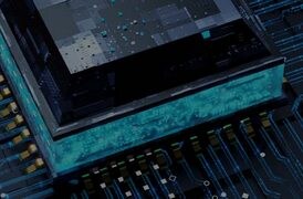
Semiconductor Device Packaging
Advanced semiconductor device packaging requires new integration approaches and innovation in performance, power efficiency, area, and cost. See how Thermo Scientific failure analysis workflows provide fast, precise, and accurate time-to-data for device packaging development.
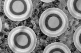
Semiconductor Pathfinding and Research
Advanced electron microscopy, focused ion beam, and associated analytical techniques for identifying viable solutions and design methods for the fabrication of high-performance semiconductor devices.
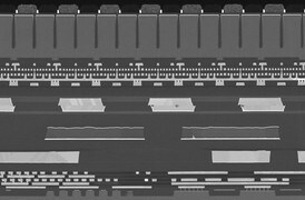
Semiconductor Failure Analysis
Increasingly complex semiconductor device structures result in more places for failure-inducing defects to hide. Our next-generation workflows help you localize and characterize subtle electrical issues that affect yield, performance, and reliability.

Physical and Chemical Characterization
Ongoing consumer demand drives the creation of smaller, faster, and cheaper electronic devices. Their production relies on high-productivity instruments and workflows that image, analyze, and characterize a broad range of semiconductor and display devices.
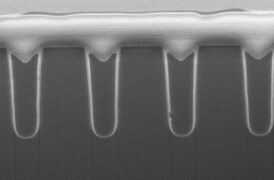
Power Semiconductor Device Analysis
Power devices pose unique challenges for localizing faults, primarily as a result of power device architecture and layout. Our power device analysis tools and workflows quickly pinpoint fault locations at operating conditions and provide precise, high-throughput analysis for characterization of materials, interfaces and device structures.

Display Module Failure Analysis
Evolving display technologies aim to improve display quality and light conversion efficiency to support applications in different industry sectors, while continuing to reduce production costs. Our process metrology, failure analysis and research and development solutions help display companies solve these challenges.
Yield Ramp and Metrology
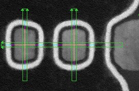
We offer advanced analytical capabilities for defect analysis, metrology, and process control, designed to help increase productivity and improve yield across a range of semiconductor applications and devices.
Semiconductor Materials and Device Characterization
As semiconductor devices shrink and become more complex, new designs and structures are needed. High-productivity 3D analysis workflows can shorten device development time, maximize yield, and ensure that devices meet the future needs of the industry.
Electron microscopy services for
semiconductors
To ensure optimal system performance, we provide you access to a world-class network of field service experts, technical support, and certified spare parts.


