Search Thermo Fisher Scientific
Auto Slice & View Software for FIB tomography
Thermo Scientific Auto Slice & View 5 (AS&V5) Software allows for automated acquisition of high-resolution 3D images and analytical maps such as EBSD (electron backscatter diffraction) or EDS (energy-dispersive X-ray spectroscopy). AS&V5 Software acquires data by milling serial sections (slices) of a sample with a focused ion beam (FIB) and then imaging and/or mapping each slice. Due to the high value and unique nature of many samples, it is important to collect as much information as possible from each section. AS&V5 Software allows you to acquire multiple imaging and analysis modalities for every slice, including information such as material and channeling contrast generated by multiple SEM and FIB detectors. Additionally, elemental information can be collected with EDS, and grain orientation/strain-texture analysis can be provided by EBSD mapping.
Spin Mill functionality
Spin Mill Science is an add-on for Auto Slice & View 5 Software that enables site-specific large area polishing and 3D characterization. Available on PFIBs and Hydra DualBeams, this software automates sequential milling and imaging of areas up to 1 mm.

Auto Slice & View Software features
Intuitive, easy to use UI
Streamlined workflows, milling recipes, integrated auto functions.
Digital tilt-shift compensation
Improve collection efficiency and accuracy.
On-the-fly editing capabilities
Adjust parameters as needed if encountering phase/microstructural change.
Integrated imaging
Integrates SEM and FIB imaging, EBSD and EDS mapping into one package.
Information on every slice
Acquire all the information on every slice (imaging, analytics, current, voltage, tilt, etc.).
Highly flexible and reliable acquisition
Highly flexible and reliable acquisition with precise and repeatable cut placement.
High speed and throughput
High speed and throughput with multi-site capability.


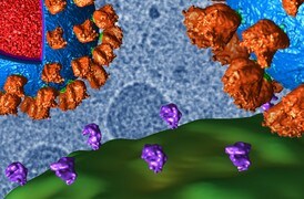
Structural Biology Research
Cryo-electron microscopy enables the structural analysis of challenging biological targets such as large complexes, flexible species and membrane protein.
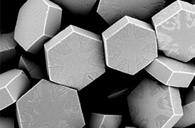
Fundamental Materials Research
Novel materials are investigated at increasingly smaller scales for maximum control of their physical and chemical properties. Electron microscopy provides researchers with key insight into a wide variety of material characteristics at the micro- to nano-scale.
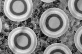
Semiconductor Pathfinding and Research
Advanced electron microscopy, focused ion beam, and associated analytical techniques for identifying viable solutions and design methods for the fabrication of high-performance semiconductor devices.
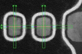
Yield Ramp and Metrology
We offer advanced analytical capabilities for defect analysis, metrology, and process control, designed to help increase productivity and improve yield across a range of semiconductor applications and devices.
Semiconductor Failure Analysis
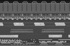
Increasingly complex semiconductor device structures result in more places for failure-inducing defects to hide. Our next-generation workflows help you localize and characterize subtle electrical issues that affect yield, performance, and reliability.

Physical and Chemical Characterization
Ongoing consumer demand drives the creation of smaller, faster, and cheaper electronic devices. Their production relies on high-productivity instruments and workflows that image, analyze, and characterize a broad range of semiconductor and display devices.

Cryo-Tomography
Cryo-electron tomography (cryo-ET) delivers both structural information about individual proteins as well as their spatial arrangements within the cell. This makes it a truly unique technique and also explains why the method has such an enormous potential for cell biology. Cryo-ET can bridge the gap between light microscopy and near-atomic-resolution techniques like single-particle analysis.

3D Materials Characterization
Development of materials often requires multi-scale 3D characterization. DualBeam instruments enable serial sectioning of large volumes and subsequent SEM imaging at nanometer scale, which can be processed into high-quality 3D reconstructions of the sample.

Cross-sectioning
Cross sectioning provides extra insight by revealing sub-surface information. DualBeam instruments feature superior focused ion beam columns for high-quality cross sectioning. With automation, unattended high-throughput processing of samples is possible.

In Situ experimentation
Direct, real-time observation of microstructural changes with electron microscopy is necessary to understand the underlying principles of dynamic processes such as recrystallization, grain growth, and phase transformation during heating, cooling, and wetting.

Multi-scale analysis
Novel materials must be analyzed at ever higher resolution while retaining the larger context of the sample. Multi-scale analysis allows for the correlation of various imaging tools and modalities such as X-ray microCT, DualBeam, Laser PFIB, SEM and TEM.
Semiconductor Analysis and Imaging
Thermo Fisher Scientific offers scanning electron microscopes for every function of a semiconductor lab, from general imaging tasks to advanced failure analysis techniques requiring precise voltage-contrast measurements.

Cryo-Tomography
Cryo-electron tomography (cryo-ET) delivers both structural information about individual proteins as well as their spatial arrangements within the cell. This makes it a truly unique technique and also explains why the method has such an enormous potential for cell biology. Cryo-ET can bridge the gap between light microscopy and near-atomic-resolution techniques like single-particle analysis.

3D Materials Characterization
Development of materials often requires multi-scale 3D characterization. DualBeam instruments enable serial sectioning of large volumes and subsequent SEM imaging at nanometer scale, which can be processed into high-quality 3D reconstructions of the sample.

Cross-sectioning
Cross sectioning provides extra insight by revealing sub-surface information. DualBeam instruments feature superior focused ion beam columns for high-quality cross sectioning. With automation, unattended high-throughput processing of samples is possible.

In Situ experimentation
Direct, real-time observation of microstructural changes with electron microscopy is necessary to understand the underlying principles of dynamic processes such as recrystallization, grain growth, and phase transformation during heating, cooling, and wetting.

Multi-scale analysis
Novel materials must be analyzed at ever higher resolution while retaining the larger context of the sample. Multi-scale analysis allows for the correlation of various imaging tools and modalities such as X-ray microCT, DualBeam, Laser PFIB, SEM and TEM.
Semiconductor Analysis and Imaging
Thermo Fisher Scientific offers scanning electron microscopes for every function of a semiconductor lab, from general imaging tasks to advanced failure analysis techniques requiring precise voltage-contrast measurements.
Electron microscopy services
To ensure optimal system performance, we provide you access to a world-class network of field service experts, technical support, and certified spare parts.


