Search Thermo Fisher Scientific
- Contact Us
- Quick Order
-
Don't have an account ? Create Account
Search Thermo Fisher Scientific
Thermo Scientific Maps Software is an imaging and correlative workflow software suite compatible with the full line of Thermo Scientific SEM, DualBeam (FIB SEM) and TEM platforms.
Scientists and researchers rely increasingly on nanoscale observations to inform the latest advances in research and analysis. It has, however, become apparent that high-resolution observations lose much of their utility in the absence of the larger macroscopic context. Observations from multiple sources must be linked, providing the necessary multi-scale and multi-modal insight for truly valuable data.
Maps Software provides a powerful imaging workflow automation package within an easy-to-use and robust platform. With just a few clicks, you can collect impactful data while preserving the context of your observations.
Whether its scanning electron microscopy analysis in SEM and DualBeam tools or transmission electron microscopy (TEM), Maps Software enables automated 2D imaging for a variety of applications, from acquiring large image mosaics to scheduling routine imaging tasks for off times (overnight, weekends).
With the ability to correlate optical and electron microscope data and easy navigation from SEM to TEM, Maps Software allows you to obtain the necessary context that drives your research and development. Use multi-modal data to aid in interpretation and navigation, ensuring you are always collecting the right data from the right location.
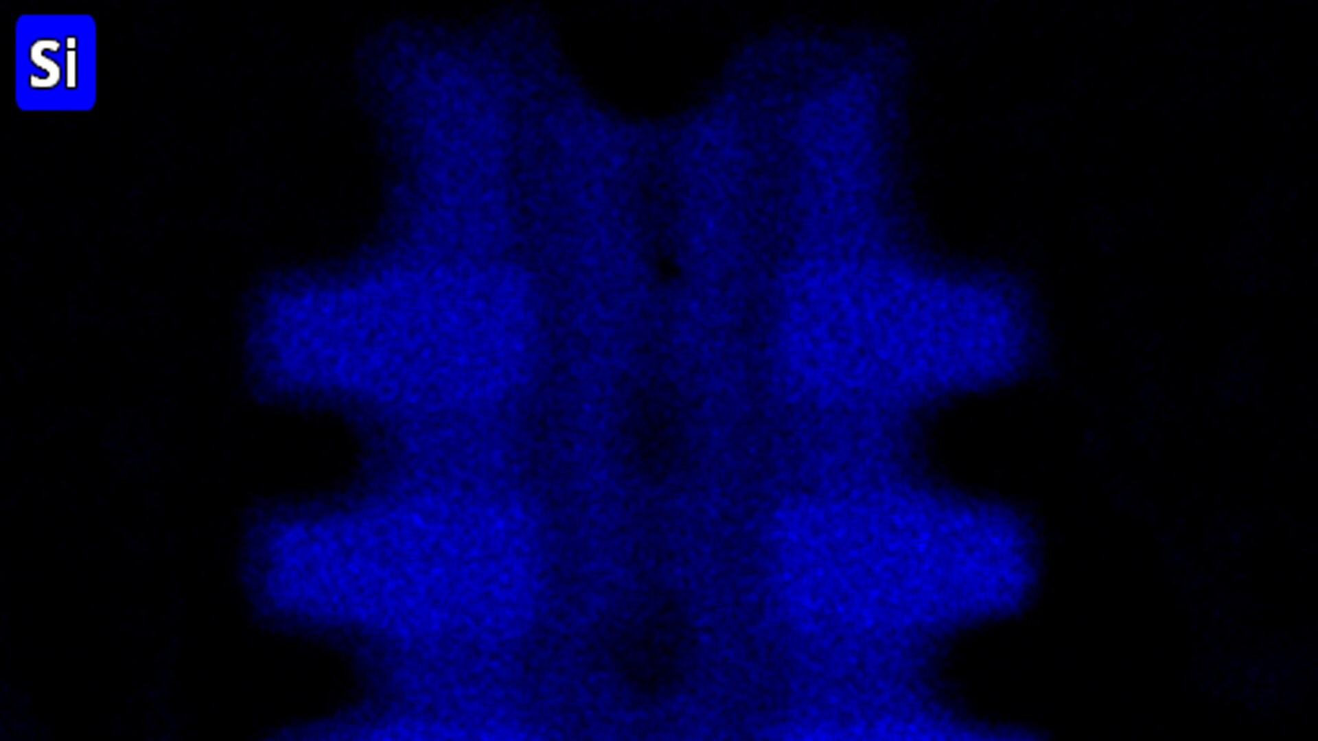
Maps Software supports integrated EDS map acquisition on STEM platforms for chemical characterization and elemental analysis along with your high-resolution imaging.
The optional offline version of Maps Software lets you take the microscope with you when you are away from the lab.
The addition of Thermo Scientific Avizo Software automates your image processing and statistical data generation. Avizo Software provides a rich, integrated user experience that blends acquisition with advanced analysis, and works in the background to process images as they are acquired.
A completely automated solution for generating high-quality, multi-scale images.
Gain insight by integrating observations across modalities and imaging platforms.
Make EDS mapping easier and instantly valuable via direct acquisition and integration of elemental layers.
The optional offline version of Maps Software allows you to continue your investigation and plan your next imaging session while away from the microscope.
This free, standalone application allows you to view Maps project from your PC (Windows 7 or 10). After installation, simply launch the application and import your projects for viewing.
Maps Offline Viewer allows you to open Maps projects on any PC. It also allows easier sharing of results without requiring a licensed version of Maps. Note that the viewer does not, however, allow processing steps like stitching, etc.
Download Maps offline viewer v3 ›
For users with images created using Maps version 3.0 or higher
Download Maps offline viewer v2 ›
For users with images created using Maps version 2.5 or lower
In this webinar, you will:
In this webinar, you will:
Cryo-EM techniques enable multiscale observations of 3D biological structures in their near-native states, informing faster, more efficient development of therapeutics.
Learn how to take advantage of rational drug design for many major drug target classes, leading to best-in-class drugs.
Fundamental plant biology research is enabled by cryo electron microscopy, which provides information on proteins (with single particle analysis), to their cellular context (with tomography), all the way up to the overall structure of the plant (large volume analysis).
Transmission electron microscopy (TEM) is used when the nature of the disease cannot be established via alternative methods. With nano-biological imaging, TEM provides accurate and reliable insight for certain pathologies.
Modern industry demands high throughput with superior quality, a balance that is maintained through robust process control. SEM and TEM tools with dedicated automation software provide rapid, multi-scale information for process monitoring and improvement.
Quality control and assurance are essential in modern industry. We offer a range of EM and spectroscopy tools for multi-scale and multi-modal analysis of defects, allowing you to make reliable and informed decisions for process control and improvement.
Novel materials are investigated at increasingly smaller scales for maximum control of their physical and chemical properties. Electron microscopy provides researchers with key insight into a wide variety of material characteristics at the micro- to nano-scale.
Innovation starts with research and development. Learn more about solutions to help you understand innovative structures and materials at the atomic level.
Manufacturing today’s complex semiconductors requires exact process controls. Learn more about advanced metrology and analysis solutions to accelerate yield learnings.
Complex semiconductor device structures result in more places for defects to hide. Learn more about failure analysis solutions to isolate, analyze, and repair defects.
Many factors impact yield, performance, and reliability. Learn more about solutions to characterize physical, structural, and chemical properties.

Single Particle Analysis
Single particle analysis (SPA) is a cryo-electron microscopy technique that enables structural characterization at near-atomic resolutions, unraveling dynamic biological processes and the structure of biomolecular complexes/assemblies.

Cryo-Tomography
Cryo-electron tomography (cryo-ET) delivers both structural information about individual proteins as well as their spatial arrangements within the cell. This makes it a truly unique technique and also explains why the method has such an enormous potential for cell biology. Cryo-ET can bridge the gap between light microscopy and near-atomic-resolution techniques like single-particle analysis.

MicroED
MicroED is an exciting new technique with applications in the structural determination of small molecules and protein. With this method, atomic details can be extracted from individual nanocrystals (<200 nm in size), even in a heterogeneous mixture.

Particle analysis
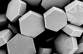
Particle analysis plays a vital role in nanomaterials research and quality control. The nanometer-scale resolution and superior imaging of electron microscopy can be combined with specialized software for rapid characterization of powders and particles.
_Technique_800x375_144DPI.jpg)
3D EDS Tomography
Modern materials research is increasingly reliant on nanoscale analysis in three dimensions. 3D characterization, including compositional data for full chemical and structural context, is possible with 3D EM and energy dispersive X-ray spectroscopy.
_Technique_800x375_144DPI.jpg)
EDS Elemental Analysis
Thermo Scientific Phenom Elemental Mapping Software provides fast and reliable information on the distribution of chemical elements within a sample.
Semiconductor TEM Imaging and Analysis
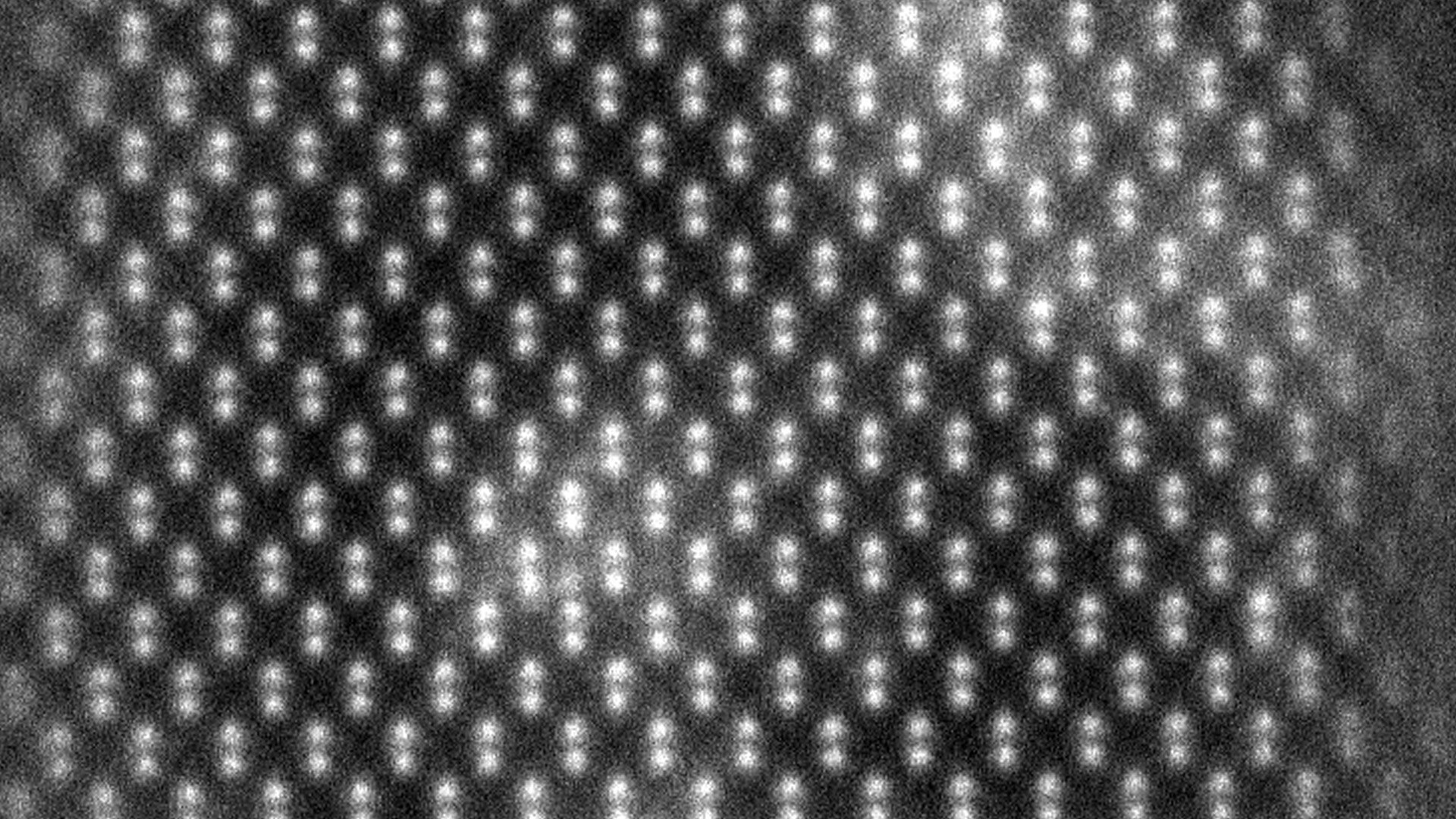
Thermo Scientific transmission electron microscopes offer high-resolution imaging and analysis of semiconductor devices, enabling manufacturers to calibrate toolsets, diagnose failure mechanisms, and optimize overall process yields.
Semiconductor Analysis and Imaging
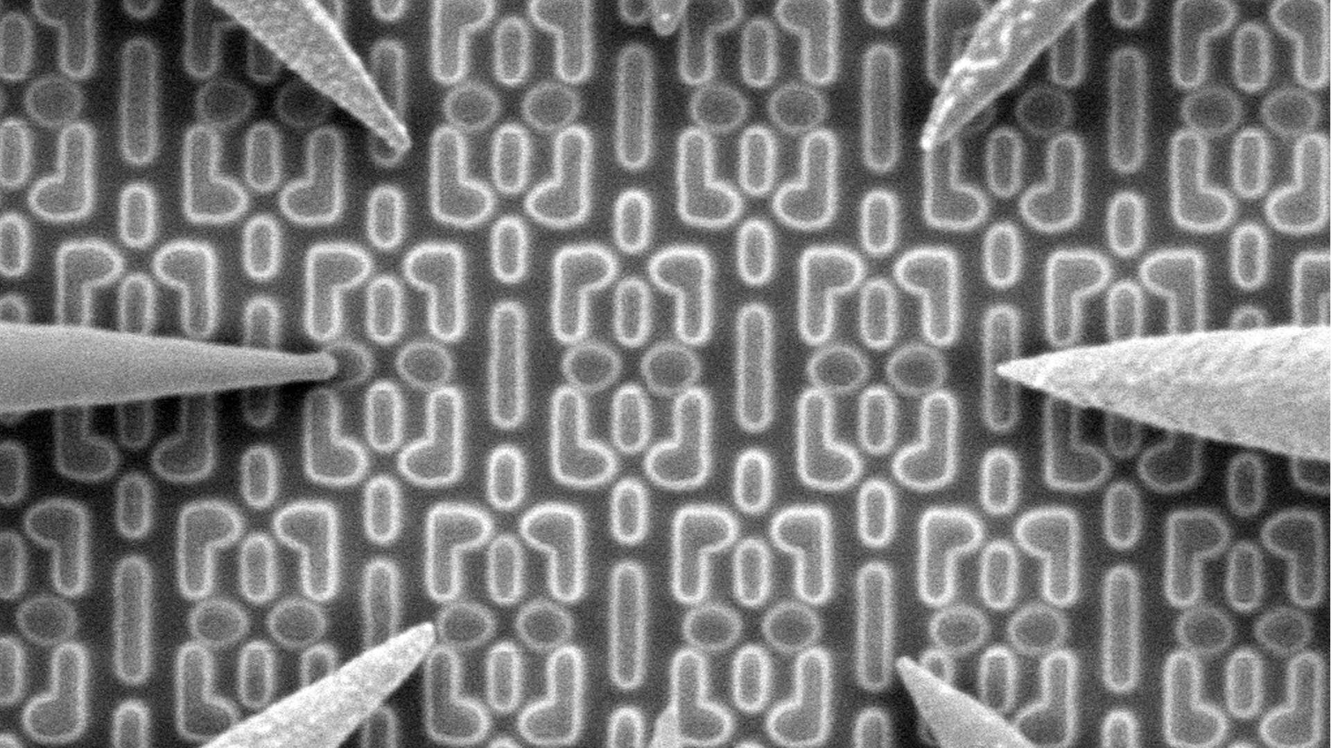
Thermo Fisher Scientific offers scanning electron microscopes for every function of a semiconductor lab, from general imaging tasks to advanced failure analysis techniques requiring precise voltage-contrast measurements.

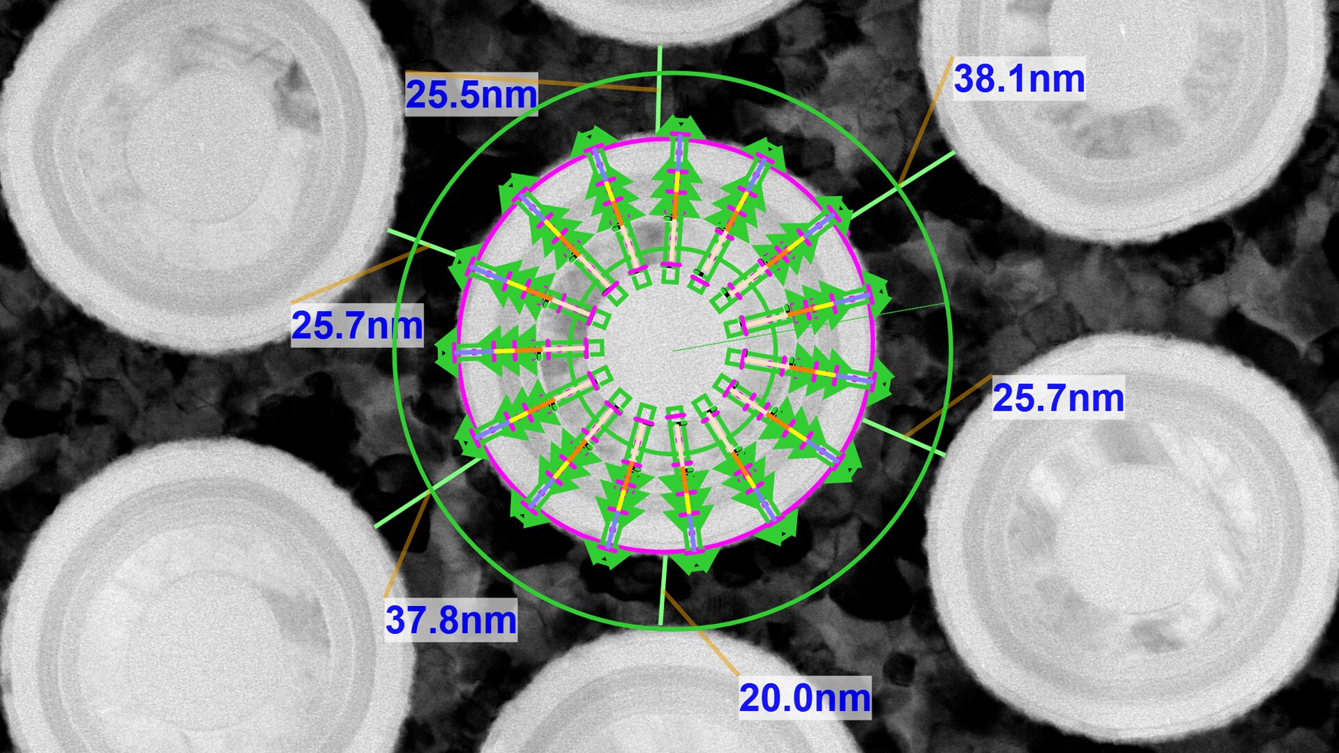
The Automated NanoParticle Workflow (APW) is a transmission electron microscope workflow for nanoparticle analysis, offering large area, high resolution imaging and data acquisition at the nanoscale, with on-the-fly processing.

Single Particle Analysis
Single particle analysis (SPA) is a cryo-electron microscopy technique that enables structural characterization at near-atomic resolutions, unraveling dynamic biological processes and the structure of biomolecular complexes/assemblies.

Cryo-Tomography
Cryo-electron tomography (cryo-ET) delivers both structural information about individual proteins as well as their spatial arrangements within the cell. This makes it a truly unique technique and also explains why the method has such an enormous potential for cell biology. Cryo-ET can bridge the gap between light microscopy and near-atomic-resolution techniques like single-particle analysis.

MicroED
MicroED is an exciting new technique with applications in the structural determination of small molecules and protein. With this method, atomic details can be extracted from individual nanocrystals (<200 nm in size), even in a heterogeneous mixture.

Particle analysis
Particle analysis plays a vital role in nanomaterials research and quality control. The nanometer-scale resolution and superior imaging of electron microscopy can be combined with specialized software for rapid characterization of powders and particles.
_Technique_800x375_144DPI.jpg)
3D EDS Tomography
Modern materials research is increasingly reliant on nanoscale analysis in three dimensions. 3D characterization, including compositional data for full chemical and structural context, is possible with 3D EM and energy dispersive X-ray spectroscopy.
_Technique_800x375_144DPI.jpg)
EDS Elemental Analysis
Thermo Scientific Phenom Elemental Mapping Software provides fast and reliable information on the distribution of chemical elements within a sample.
Semiconductor TEM Imaging and Analysis
Thermo Scientific transmission electron microscopes offer high-resolution imaging and analysis of semiconductor devices, enabling manufacturers to calibrate toolsets, diagnose failure mechanisms, and optimize overall process yields.
Semiconductor Analysis and Imaging
Thermo Fisher Scientific offers scanning electron microscopes for every function of a semiconductor lab, from general imaging tasks to advanced failure analysis techniques requiring precise voltage-contrast measurements.

The Automated NanoParticle Workflow (APW) is a transmission electron microscope workflow for nanoparticle analysis, offering large area, high resolution imaging and data acquisition at the nanoscale, with on-the-fly processing.
To ensure optimal system performance, we provide you access to a world-class network of field service experts, technical support, and certified spare parts.


