Search Thermo Fisher Scientific
- Contact Us
- Quick Order
-
Don't have an account ? Create Account
Search Thermo Fisher Scientific
A major, ongoing challenge of the tech industry is the shrinking of semiconductor devices and transistor feature dimensions. To maintain excellent reliability, performance, and yield, semiconductor failure analysis techniques have to constantly improve in order to meet this challenge. As a result, high-end, advanced instrumentation is needed to localize and identify defective structures, which have more places to hide due to high-density interconnects, wafer-level stacking, and complex 3D architectures.
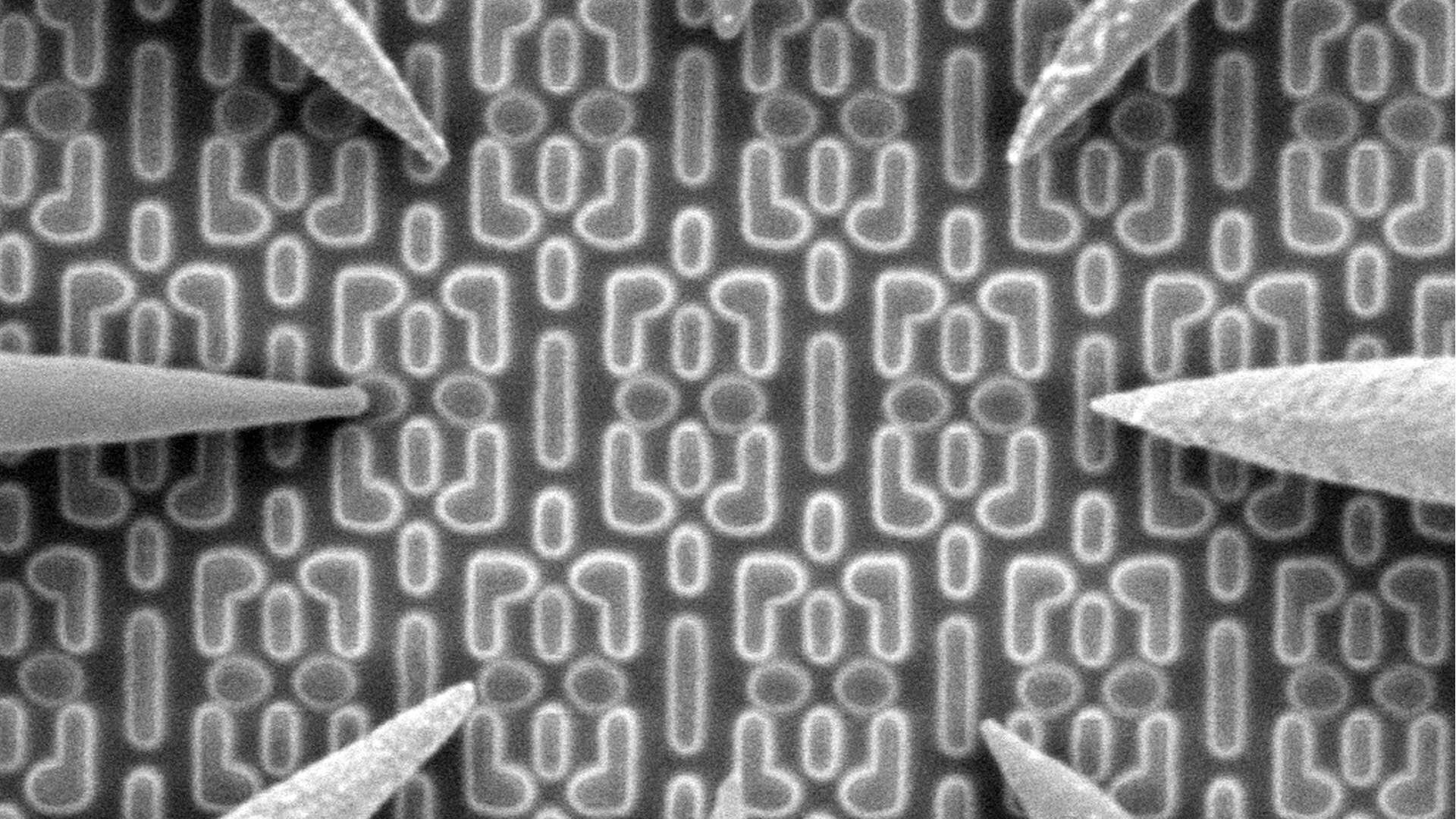
Nanoprobing is an advanced characterization technique designed to isolate electrical defects that can negatively influence yield, reliability, and performance. Nanoprobing also provides the precise localization of electrical faults, which is necessary for an effective transmission electron microscopy (TEM) failure analysis workflow.
Thermo Fisher Scientific provides a range of advanced nanoprobing and sample preparation tools for reliable and accurate electrical fault isolation on a wide range of advanced devices. The Thermo Scientific nProber IV System is a high-performance scanning-electron-microscopy-based platform for the localization of transistor and metallization faults. The Thermo Scientific Hyperion II System is a high-productivity atomic-force-profiling nanoprober, with leading-edge transistor-probing performance that includes integrated conductive atomic force microscopy (C-AFM) capability. See the product pages below for more information.
Performance, power efficiency, area, and cost are driving packaging innovations. Learn how workflows provide fast, precise, and accurate time-to-data.
Complex semiconductor device structures result in more places for defects to hide. Learn more about failure analysis solutions to isolate, analyze, and repair defects.
Many factors impact yield, performance, and reliability. Learn more about solutions to characterize physical, structural, and chemical properties.
Every electrostatic discharge (ESD) control plan is required to identify devices that are sensitive to ESD. We offer a complete suite of test systems to help with your device qualification requirements.
Novel architectures and materials pose new challenges. Learn how to pinpoint faults and characterize materials, structures, and interfaces.
Innovation starts with research and development. Learn more about solutions to help you understand innovative structures and materials at the atomic level.
As semiconductor devices shrink and become more complex, new designs and structures are needed. High-productivity 3D analysis workflows can shorten device development time, maximize yield, and ensure that devices meet the future needs of the industry.
To ensure optimal system performance, we provide you access to a world-class network of field service experts, technical support, and certified spare parts.
