Search Thermo Fisher Scientific
Demand for faster, smaller, and more interconnected devices continues to drive atomic scale technology developments. Researchers and engineers need reliable and rapid analysis and characterization at these dimensions, which only transmission electron microscopy (TEM) can provide.
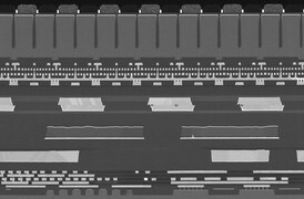
The Thermo Scientific Talos F200E (Scanning) Transmission Electron Microscope provides high-resolution STEM and TEM imaging with minimal distortion, combined with high-throughput energy-dispersive X-ray spectroscopy (EDS) functionality, tailored for a wide range of semiconductor defect analysis and research applications.
A high-productivity solution for semiconductor and microelectronics analysis
Supporting the fast pace of process development and yield ramp significantly strains semiconductor analysis labs, as they must provide repeatable, high-resolution characterization of a wide variety of materials and devices. The Talos F200E (S)TEM was designed with these labs in mind, delivering >1.5× faster EDS analysis compared to previous Talos models and ≤1% TEM image distortion. The speed and repeatability improvements make the Talos F200E (S)TEM the industry choice for device analysis, defect characterization, and yield support.
High-quality (S)TEM imaging
High-throughput TEM imaging with minimized distortion and simultaneous, multiple-signal detection, and contrast-optimized STEM imaging.
Precise, high-speed chemical characterization
Rapid, precise, qualitative or quantitative EDS acquisition and analysis.
Dedicated semiconductor-related applications
Includes: specimen-stage-synchronized live TEM image rotation, simultaneous operation of multiple STEM detectors, integrated differential phase contrast (iDPC) imaging, STEM field-of-view matching, instant EDS map quantification, minimized image distortion, and more.
| Brightness of X-FEG | 1.8 × 10⁹ A/cm2 srad (@200 kV) | |
| Total beam current | > 50 nA | |
| EDS system | Super-X | Dual-X |
| Full solid angle | 0.9 srad | 2.56 srad |
| Effective solid angle* | 0.9 srad | 1.65 srad |
| Detectors | 4 SDD | 2 larger SDD |
| Camera | Low-distortion 4k × 4k with the Thermo Scientific Ceta-M Camera | |
| STEM | Panther STEM segment detectors | |
| SEMI S2 | Certified | |
| STEM resolution | ≤0.16 nm | |
| TEM information limit | ≤0.12 nm | |
| TEM line resolution | ≤0.10 nm | |
| Max. diffraction angle | 24˚ | |
| Z-movement | ±0.375 mm | |
| TEM image linear distortion | ≤1% | |
| TEM image variation(optional) | ≤1% | |
| Gatan Continuum Filter | Optional | |

Análise de falha de semicondutores
Estruturas de dispositivos semicondutores cada vez mais complexas resultam em mais locais onde defeitos que induzem falhas podem se ocultar. Nossos fluxos de trabalho de última geração o ajudam a localizar e caracterizar problemas elétricos sutis que afetam o rendimento, o desempenho e a confiabilidade.

Caracterização física e química
A demanda contínua dos consumidores impulsiona a criação de dispositivos eletrônicos menores, mais rápidos e mais baratos. Sua produção depende de instrumentos e fluxos de trabalho de alta produtividade que fazem imagens, analisam e caracterizam uma ampla gama de semicondutores e dispositivos de exibição.
