Search Thermo Fisher Scientific

Spectra 200 Scanning Transmission Electron Microscope
For scientists to advance their understanding of complex samples and develop innovative materials, they must have access to robust, precise instrumentation capable of correlating form and function, as well as resolving space, time and frequency.
Thermo Fisher Scientific introduces the Thermo Scientific Spectra 200 (S)TEM, the high-throughput, aberration-corrected, (scanning) transmission electron microscope for all materials science applications.
Spectra 200 Scanning Transmission Electron Microscope advantages
All Spectra 200 (S)TEM's are delivered on new platforms designed to offer an unprecedented level of mechanical stability and highest imaging quality though passive and (optional) active vibration isolation.
The system is housed in a fully re-designed enclosure with a built-in on-screen display for convenient specimen loading and removal. For the first time, full modularity and upgradeability can be offered between uncorrected and single-corrected configurations with variable heights, allowing maximum flexibility for different room configurations.
The Spectra 200 (S)TEM can be powered by a new-cold field emission gun (X-CFEG). The X-CFEG has extremely high brightness (>>1.0 x 10⁸ A/m2/Sr/V*), low energy spread, and can be operated from 30 – 200 kV. This provides high-resolution STEM imaging with high probe currents for high-throughput, fast acquisition STEM analytics. With the powerful combination of X-CFEG and S-CORR probe aberration corrector, sub-Angstrom STEM imaging with over 1000 pA of probe current can be routinely achieved.
 images of silicon.")
Si[110] HAADF images taken on a Spectra 200 S/TEM with probe currents ranging from 0.016 nA up to 1 nA while maintaining <76 pm STEM resolution.
Further, probe currents can be flexibly tuned from <1 pA up to the nA range with fine control of the gun and condenser optics, all with minimum impact on the probe aberrations, so that the widest range of specimens and experiments can be accommodated (see the MOF example in the Panther STEM detection section).
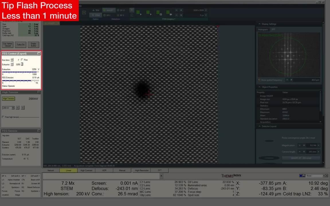
As with all cold field emission sources, the sharp tip requires a periodic regeneration (called flashing) to maintain the probe current. With the X-CFEG, the tip only requires flashing once per working day, a process that takes less than a minute. There is no measurable impact on the probe aberrations even in the highest resolution imaging conditions and the daily tip flashing process has no impact on the tip lifetime.
Tip flashing on the X-CFEG: 60 pm resolution at 200 kV is maintained before and after a tip flashing without adjustment of the optics. The process takes less than one minute and is required only once per working day and has no impact on the lifetime of the tip.
This new generation X-CFEG also produces enough total beam current (>14 nA) to support standard TEM imaging experiments (e.g. in situ) with large parallel probes, making it a uniquely all-purpose, yet high-performance, C-FEG.
The combination of enhanced mechanical stability, the latest 5th order S-CORR probe aberration correction and the X-CFEG, gives the Spectra 200 (S)TEM high-resolution, high-contrast STEM imaging capability for all accelerating voltages. Additionally, Spectra 200 (S)TEM retains the wide gap S-TWIN objective lens as standard from the Themis product line, to ensure customers have a pole gap with “room to do more” without compromising on spatial resolution. In the images below, 48 pm resolution is shown on a wide gap S-TWIN Spectra 200 (S)TEM at 200 kV.
Adding to ease of use, the Spectra 200 (S)TEM includes smart software algorithms to quickly, reproducibly and reliably correct up to 4th order aberrations in the STEM probe (Auto S-CORR) and optimize 1st and 2nd order aberrations on any specimen (OptiSTEM+). Auto S-CORR can therefore be used on a weekly basis to maintain high-order aberrations and OptiSTEM+ can be used daily to optimize image quality without the need of a standard specimen or manual tuning.
 images of GaN and silicon.")
Si [110] and GaN [212] taken on a Spectra 200 (S)TEM showing the specified resolution on a wide gap analytical S-TWIN pole piece (green circle) and achievable resolution (red circles). At 60 kV, 96 pm resolution is specified and at 200 kV, 60 pm is specified with an achievable resolution <48 pm.
The Spectra 200 (S)TEM offers STEM resolution specifications of 60 pm at 200 kV, 96 pm at 60 kV and 125 pm at 30 kV. For a full list of specifications, please refer to the Spectra 200 (S)TEM datasheet.
STEM imaging on the Spectra 200 (S)TEM has been re-imagined with the Panther STEM detection system, which includes a new data acquisition architecture and two new, solid state, eight-segment ring and disk STEM detectors (16 segments in total). The new detector geometry offers access to advanced STEM imaging capability combined with the sensitivity to measure single electrons.

The 16 segmented ring and disk detectors of the Panther STEM detection system allow for a range of STEM signals without the need for multiple detectors.
The entire signal is optimized and tuned to provide unprecedented signal-to-noise imaging capability with extremely low doses to facilitate imaging of beam sensitive materials. Additionally, the completely redeveloped data acquisition infrastructure can combine different individual detector segments, with the future possibility of combining detector segments in arbitrary ways, generating new STEM imaging methods and revealing information that is not present in conventional STEM techniques. The architecture is also scalable and provides an interface to synchronize multiple STEM and spectroscopic signals.
 images of SrTiO3.")
Comparison SrTiO₃ [001] HAADF images taken with the Panther STEM detection system with 3 pA, 1.3 pA and <1 pA of probe current. Even with probe currents <1 pA, the signal-to-noise ratio in the image allows automation routines like OptiSTEM+ to correct 1st and 2nd order aberrations in the probe forming optics, delivering sharp images.

Metal Organic Framework (MOF) MIL-101 imaged with 0.5 pA of beam current in STEM with iDPC
at 200kV. The image is a single shot with a frame time of 23.5 seconds and the complex structure can be seen with 2 Å resolution. (Specimen courtesy of Professor Y. Han, King Abdullah University of Science and Technology.)
The Spectra 200 (S)TEM can be configured with an electron microscope pixel array detector (EMPAD) or a Thermo Scientific Ceta Camera with speed enhancement to collect 4D STEM data sets.
The EMPAD is capable of 30-300 kV and provides a high dynamic range (1:1,000,000 e- between pixels), high signal-to-noise ratio (1/140 e-), and high speed (1100 frames per second) on a 128 x 128 pixel array, which makes it the optimal detector for 4D STEM applications. (E.g. Applications where the details of the central and diffracted beams need to be analyzed simultaneously, as in the ptychography image below.)
More details can be found in the EMPAD datasheet.
 image of MoS2.")
The EMPAD detector can be used for a wide variety of applications. On the left, it is used to extend spatial resolution (0.39 Å) beyond the aperture limited resolution at low accelerating voltages (80 kV) in a bi-layer of the 2D material MoS2 ( Jiang, Y. et al. Nature 559, 343–349, 2018) . On the right, it is used to independently image dark field reflections, revealing the complex microstructure of the precipitates in a superalloy (Sample courtesy Professor G. Burke, University of Manchester).
The Ceta Camera with speed enhancement offers an alternative for 4D STEM applications where a greater number of pixels is required and when EDX analysis needs to be combined with each point in the STEM scan. This solution provides higher resolution diffraction patterns (up to 512 x 512 pixel resolution), suited for applications such as strain measurement.
The Spectra 200 (S)TEM has been configured to be a STEM analytics powerhouse. The extreme brightness and low energy spread of the X-CFEG, the latest generation, 5th order S-CORR probe corrector, the wide gap (S-TWIN or X-TWIN) pole piece with a portfolio of large solid angle and symmetric EDS detectors and the built-in EDX quantification engine in Thermo Scientific Velox Software makes STEM EDX on Spectra 200 (S)TEM fast, easy and quantifiable.
The Thermo Scientific EDX detector portfolio provides a choice of detector geometries to suit your experimental requirements and optimize EDX results. Both configurations have a symmetric design (see below), producing quantifiable data. Note that holder shadowing as a function of tilt is compensated in both detector configurations via built-in Velox Software functionality.
The Spectra 200 (S)TEM can be configured with either Super-X (for spectrum cleanliness and quantification) or Dual-X (for the largest solid angle and high-throughput STEM EDX mapping).
The Super-X detector system provides a highly collimated solid angle of 0.7 Sr and a Fiori number greater than 4000. It is designed for STEM EDX experiments where spectral cleanliness and quantification are critical.
The Dual-X detector system provides a solid angle of 1.76 Sr and a Fiori number greater than 2000. It is designed for high-throughput STEM EDX experiments such as EDS tomography or where signal yield is low and fast mapping is critical.
In the example below, the DyScO3 perovskite system is examined with the Dual-X detectors. The ultra-high brightness (>>1.0 x 10⁸ A/m2/Sr/V*) of the X-CFEG and the resolving power of the S-CORR probe corrector are used to deliver a probe to the specimen with 150 pA of current and size <80 pm. With these high-brightness probe conditions, EDX mapping can be done rapidly with high sampling and high SNR, resulting in, for the first time, sub-Å spatial information in a single elemental, raw, and unfiltered EDX map. A fast Fourier transform of the Sc map shows up to 90 pm resolution.

DyScO3 specimen investigated with the powerful combination of ultra-high brightness X-CFEG, S-CORR and the large solid angle (1.76 Sr) of the Dual-X detectors, resulting in high signal-to-noise ratio, atomic resolution (up to 90 pm), unfiltered EDX maps (Sample courtesy Professor L.F. Kourkoutis, Cornell University).
Electron energy loss spectroscopy on Spectra 200 (S)TEM has also been accelerated by the ultra-high brightness (>>1.0 x 10⁸ A/m2/Sr/V*) and intrinsically high energy resolution (<0.4 eV) of the X-CFEG which are delivered simultaneously in the STEM probe.
In the figure below, a probe with narrow energy spread (0.36 eV) and high current (480 pA) high spatial resolution (65 pm) provides ideal conditions to collect the Dy, Sc and O core loss edges with high energy resolution, signal to noise ratio and spatial resolution in the STEM image.

DyScO3 specimen investigated with a Spectra 200 (S)TEM. The combined ultra-high brightness of the X-CFEG, intrinsically low energy spread of the source (<0.40 eV) and resolving power of the S-CORR results in high signal-to-noise ratio, Sc, O and Dy core loss edges with a sub-70 pm STEM probe (Sample courtesy Professor L.F. Kourkoutis, Cornell University).
Folha de estilo para especificações de tabela de produtos
| Spectra 200 (S)TEM |
|
| Source |
|
| Analytics and detectors |
|
| Available detector options |
|
Style Sheet for Komodo Tabs
 images of silicon.")
Si[110] HAADF images taken on a Spectra 200 (S)TEM with probe currents ranging from 0.016 nA up to 1 nA while maintaining <76 pm STEM resolution.
 images of GaN and silicon.")
Si [110] and GaN [212] taken on a Spectra 200 (S)TEM showing the specified resolution on a wide gap analytical S-TWIN pole piece (green circle) and achievable resolution (red circles). At 60 kV, 96 pm resolution is specified and at 200 kV, 60 pm is specified with an achievable resolution <48 pm.

The 16 segmented ring and disk detectors of the Panther STEM detection system allow for a range of STEM signals without the need for multiple detectors.
 images of SrTiO₃.")
Comparison SrTiO₃ [001] HAADF images taken with the Panther STEM detection system with 3 pA, 1.3 pA and <1 pA of probe current. Even with probe currents <1 pA, the signal-to-noise ratio in the image allows automation routines like OptiSTEM+ to correct 1st and 2nd order aberrations in the probe forming optics, delivering sharp images.

Metal Organic Framework (MOF) MIL-101 imaged with 0.5 pA of beam current in STEM with iDPC at 200kV. The image is a single shot with a frame time of 23.5 seconds and the complex structure can be seen with 2 Å resolution. (Specimen courtesy of Professor Y. Han, King Abdullah University of Science and Technology.)
 image of MoS₂.")
The EMPAD detector can be used for a wide variety of applications. On the left, it is used to extend spatial resolution (0.39 Å) beyond the aperture limited resolution at low accelerating voltages (80 kV) in a bi-layer of the 2D material MoS₂ (Jiang, Y. et al. Nature 559, 343–349, 2018). On the right, it is used to independently image dark field reflections, revealing the complex microstructure of the precipitates in a superalloy (Sample courtesy Professor G. Burke, University of Manchester).

DyScO₃ specimen investigated with the powerful combination of ultra-high brightness X-CFEG, S-CORR and the large solid angle (1.76 Sr) of the Dual-X detectors, resulting in high signal-to-noise ratio, atomic resolution (up to 90 pm), unfiltered EDX maps (Sample courtesy Professor L.F. Kourkoutis, Cornell University).

DyScO₃ specimen investigated with a Spectra 200 (S)TEM. The combined ultra-high brightness of the X-CFEG, intrinsically low energy spread of the source (<0.40 eV) and resolving power of the S-CORR results in high signal-to-noise ratio, Sc, O and Dy core loss edges with a sub-70 pm STEM probe (Sample courtesy Professor L.F. Kourkoutis, Cornell University).
Tip flashing on the X-CFEG: 60 pm resolution at 200 kV is maintained before and after a tip flashing without adjustment of the optics. The process takes < 1 min, and is required only once per working day and has no impact on the lifetime of the tip.
The Spectra 200 (S)TEM can be configured with Dual-X for the largest solid angle and high-throughput STEM EDX mapping.
The Spectra 200 (S)TEM can be configured with Super-X for spectrum cleanliness and quantification.
TEM")
Introducing the Spectra 200 (S)TEM
Thermo Fisher Scientific introduces the Spectra 200 (S)TEM – the high-throughput, aberration-corrected, scanning transmission electron microscope for all materials science applications.
Register below to watch our recorded webinar and learn more about how the Spectra 200 (S)TEM delivers the highest-quality data for all applications. With an ultra-high-brightness X-CFEG source and a wide-gap pole piece with “room to do more,” it is the ultimate atomic-resolution materials-characterization tool.
Si[110] HAADF images taken on a Spectra 200 (S)TEM with probe currents ranging from 0.016 nA up to 1 nA while maintaining <76 pm STEM resolution.
Si [110] and GaN [212] taken on a Spectra 200 (S)TEM showing the specified resolution on a wide gap analytical S-TWIN pole piece (green circle) and achievable resolution (red circles). At 60 kV, 96 pm resolution is specified and at 200 kV, 60 pm is specified with an achievable resolution <48 pm.
The 16 segmented ring and disk detectors of the Panther STEM detection system allow for a range of STEM signals without the need for multiple detectors.
Comparison SrTiO₃ [001] HAADF images taken with the Panther STEM detection system with 3 pA, 1.3 pA and <1 pA of probe current. Even with probe currents <1 pA, the signal-to-noise ratio in the image allows automation routines like OptiSTEM+ to correct 1st and 2nd order aberrations in the probe forming optics, delivering sharp images.
Metal Organic Framework (MOF) MIL-101 imaged with 0.5 pA of beam current in STEM with iDPC at 200kV. The image is a single shot with a frame time of 23.5 seconds and the complex structure can be seen with 2 Å resolution. (Specimen courtesy of Professor Y. Han, King Abdullah University of Science and Technology.)
The EMPAD detector can be used for a wide variety of applications. On the left, it is used to extend spatial resolution (0.39 Å) beyond the aperture limited resolution at low accelerating voltages (80 kV) in a bi-layer of the 2D material MoS₂ (Jiang, Y. et al. Nature 559, 343–349, 2018). On the right, it is used to independently image dark field reflections, revealing the complex microstructure of the precipitates in a superalloy (Sample courtesy Professor G. Burke, University of Manchester).
DyScO₃ specimen investigated with the powerful combination of ultra-high brightness X-CFEG, S-CORR and the large solid angle (1.76 Sr) of the Dual-X detectors, resulting in high signal-to-noise ratio, atomic resolution (up to 90 pm), unfiltered EDX maps (Sample courtesy Professor L.F. Kourkoutis, Cornell University).
DyScO₃ specimen investigated with a Spectra 200 (S)TEM. The combined ultra-high brightness of the X-CFEG, intrinsically low energy spread of the source (<0.40 eV) and resolving power of the S-CORR results in high signal-to-noise ratio, Sc, O and Dy core loss edges with a sub-70 pm STEM probe (Sample courtesy Professor L.F. Kourkoutis, Cornell University).
Tip flashing on the X-CFEG: 60 pm resolution at 200 kV is maintained before and after a tip flashing without adjustment of the optics. The process takes < 1 min, and is required only once per working day and has no impact on the lifetime of the tip.
The Spectra 200 (S)TEM can be configured with Dual-X for the largest solid angle and high-throughput STEM EDX mapping.
The Spectra 200 (S)TEM can be configured with Super-X for spectrum cleanliness and quantification.
Introducing the Spectra 200 (S)TEM
Thermo Fisher Scientific introduces the Spectra 200 (S)TEM – the high-throughput, aberration-corrected, scanning transmission electron microscope for all materials science applications.
Register below to watch our recorded webinar and learn more about how the Spectra 200 (S)TEM delivers the highest-quality data for all applications. With an ultra-high-brightness X-CFEG source and a wide-gap pole piece with “room to do more,” it is the ultimate atomic-resolution materials-characterization tool.

Controle de processo
A indústria moderna exige alta produtividade com qualidade superior, um equilíbrio mantido por meio de um controle de processo robusto. As ferramentas SEM e TEM com software de automação dedicado proporcionam informações rápidas e em várias escalas para monitoramento e aprimoramento de processos.

Controle de qualidade
O controle de qualidade e a garantia de qualidade são essenciais na indústria moderna. Oferecemos uma gama de ferramentas de microscopia eletrônica e espectroscopia para análises multidimensionais e multimodais de defeitos, permitindo que você tome decisões confiáveis e informadas para controle e melhoria de processos.

Pesquisa de materiais fundamentais
Novos materiais são investigados em escalas cada vez menores para o máximo controle de suas propriedades físicas e químicas. A microscopia eletrônica fornece aos pesquisadores percepções importantes sobre uma ampla variedade de características materiais em escala micro a nano.

Espectroscopia por energia dispersiva
A espectroscopia por energia dispersiva (EDS) coleta informações elementares detalhadas juntamente com imagens de microscopia eletrônica, fornecendo contexto de composição crítico para observações EM. Com a EDS, a composição química pode ser determinada a partir de varreduras de superfície rápidas e holísticas que chegam até a átomos individuais.
_Technique_800x375_144DPI.jpg)
Tomografia EDS 3D
A pesquisa de materiais modernos depende cada vez mais da análise nanométrica em três dimensões. A caracterização 3D, incluindo dados de composição para contexto químico e estrutural completos, é possível com a EM 3D e a espectroscopia de raios X por energia dispersiva.

Mapeamento elementar em escala atômica com EDS
A EDS de resolução atômica fornece um contexto químico sem igual para análise de materiais, diferenciando a identidade elementar de átomos individuais. Quando combinado com a TEM de alta resolução, é possível observar a organização precisa dos átomos em uma amostra.
_Technique_800x375_144DPI.jpg)
Análise elementar EDS
A EDS proporciona informações de composição vitais para observações em microscópio eletrônico. Principalmente, nossos exclusivos sistemas detectores Super-X e Dual-X adicionam opções para maior produtividade e/ou sensibilidade, permitindo otimizar a aquisição de dados para atender às prioridades de pesquisa.

Espectroscopia de perda eletrônica de energia
A pesquisa da ciência de materiais se beneficia da EELS de alta resolução para uma ampla variedade de aplicações analíticas. Isso inclui mapeamento elementar de alto rendimento, alta taxa de sinal e ruído e sondagem de estados de oxidação e fótons de superfície.

Experimentação in situ
A observação direta e em tempo real de alterações microestruturais com a microscopia eletrônica é necessária para entender os princípios subjacentes de processos dinâmicos, como recristalização, crescimento de grãos e transformação de fases durante o aquecimento, o resfriamento e a umidificação.

Análise de partículas
A análise de partículas tem uma função vital na pesquisa de nanomateriais e no controle de qualidade. A resolução nanométrica e a formação de imagens excelentes da microscopia eletrônica podem ser combinadas com software especializado proporcionando uma rápida caracterização de pós e partículas.

Análise em várias escalas
Os materiais novos precisam ser analisados em resolução cada vez maior, mantendo o contexto maior da amostra. A análise em várias escalas permite correlacionar várias ferramentas e modalidades de geração de imagens, como a microTC de raios X, DualBeam, laser PFIB, SEM e TEM.

Fluxo de trabalho de partículas automatizado
O fluxo de trabalho de nanopartículas automatizado (APW) consiste em um fluxo de trabalho de microscópio eletrônico de transmissão para análise de nanopartículas, oferecendo imagens de grande área e alta resolução e aquisição de dados nanométricos em um processamento dinâmico.
Espectroscopia por energia dispersiva
A espectroscopia por energia dispersiva (EDS) coleta informações elementares detalhadas juntamente com imagens de microscopia eletrônica, fornecendo contexto de composição crítico para observações EM. Com a EDS, a composição química pode ser determinada a partir de varreduras de superfície rápidas e holísticas que chegam até a átomos individuais.
Tomografia EDS 3D
A pesquisa de materiais modernos depende cada vez mais da análise nanométrica em três dimensões. A caracterização 3D, incluindo dados de composição para contexto químico e estrutural completos, é possível com a EM 3D e a espectroscopia de raios X por energia dispersiva.
Mapeamento elementar em escala atômica com EDS
A EDS de resolução atômica fornece um contexto químico sem igual para análise de materiais, diferenciando a identidade elementar de átomos individuais. Quando combinado com a TEM de alta resolução, é possível observar a organização precisa dos átomos em uma amostra.
Análise elementar EDS
A EDS proporciona informações de composição vitais para observações em microscópio eletrônico. Principalmente, nossos exclusivos sistemas detectores Super-X e Dual-X adicionam opções para maior produtividade e/ou sensibilidade, permitindo otimizar a aquisição de dados para atender às prioridades de pesquisa.
Espectroscopia de perda eletrônica de energia
A pesquisa da ciência de materiais se beneficia da EELS de alta resolução para uma ampla variedade de aplicações analíticas. Isso inclui mapeamento elementar de alto rendimento, alta taxa de sinal e ruído e sondagem de estados de oxidação e fótons de superfície.
Experimentação in situ
A observação direta e em tempo real de alterações microestruturais com a microscopia eletrônica é necessária para entender os princípios subjacentes de processos dinâmicos, como recristalização, crescimento de grãos e transformação de fases durante o aquecimento, o resfriamento e a umidificação.
Análise de partículas
A análise de partículas tem uma função vital na pesquisa de nanomateriais e no controle de qualidade. A resolução nanométrica e a formação de imagens excelentes da microscopia eletrônica podem ser combinadas com software especializado proporcionando uma rápida caracterização de pós e partículas.
Análise em várias escalas
Os materiais novos precisam ser analisados em resolução cada vez maior, mantendo o contexto maior da amostra. A análise em várias escalas permite correlacionar várias ferramentas e modalidades de geração de imagens, como a microTC de raios X, DualBeam, laser PFIB, SEM e TEM.
Fluxo de trabalho de partículas automatizado
O fluxo de trabalho de nanopartículas automatizado (APW) consiste em um fluxo de trabalho de microscópio eletrônico de transmissão para análise de nanopartículas, oferecendo imagens de grande área e alta resolução e aquisição de dados nanométricos em um processamento dinâmico.
Style Sheet to change H2 style to p with em-h2-header class
Serviços de microscopia eletrônica para
a ciência dos materiais
Para garantir o desempenho ideal do sistema, fornecemos acesso a uma rede de especialistas em serviços de campo, suporte técnico e peças de reposição certificadas.
Suporte e recursos para microscopia eletrônica
Folha de estilo para Rodapé de suporte e serviço
Folha de estilo para Fontes
Folha de estilo para Cartões